As seen on Hackaday!
TL;DR – The SanDisk High Endurance cards use SanDisk/Toshiba 3D TLC Flash. It took way, way more work than it should have to figure this out (thanks for nothing, SanDisk!).
In contrast, the SanDisk MAX Endurance uses the same 3D TLC in pMLC (pseudo-multi-level cell) mode.
In a previous blog post, I took a look at SanDisk’s microSD cards that were aimed for use in write-intensive applications like dash cameras. In that post I took a look at its performance metrics, and speculated about what sort of NAND Flash memory is used inside. SanDisk doesn’t publish any detailed specifications about the cards’ internal workings, so that means I have no choice but to reverse-engineer the can of worms card myself.
The Help Desk That Couldn’t
In the hopes of uncovering more information, I sent an email to SanDisk’s support team asking about what type of NAND Flash they are using in their High Endurance lineup of cards, alongside endurance metrics like P/E (Program/Erase) cycle counts and total terabytes written (TBW). Unfortunately, the SanDisk support rep couldn’t provide a satisfactory answer to my questions, as they’re not able to provide any information that’s not listed in their public spec sheets. They said that all of their cards use MLC Flash, which I guess is correct if you call TLC Flash 3-bit MLC (which Samsung does).
Dear Jason,
Thank you for contacting SanDisk® Global customer care. We really appreciate you being a part of our SanDisk® family.
I understand that you wish to know more about the SanDisk® High Endurance video monitoring card, as such please allow me to inform you that all our SanDisk® memory cards uses Multi level cell technology (MLC) flash. However, the read/write cycles for the flash memory is not published nor documented only the read and write speed in published as such they are 100 MB/S & 40 MB/s. The 64 GB card can record Full HD video up to 10,000 hours. To know more about the card you may refer to the link below:
SANDISK HIGH ENDURANCE VIDEO MONITORING microSD CARD
Best regards,
Allan B.
SanDisk® Global Customer Care
I’ll give them a silver star that says “You Tried” at least.
Anatomy of an SD Card
While (micro)SD cards feel like a solid monolithic piece of technology, they’re made up of multiple different chips, each performing a different role. A basic SD card will have a controller that manages the NAND Flash chips and communicates with the host (PC, camera, etc.), and the NAND Flash itself (made up of 1 or more Flash dies). Bunnie Huang’s blog, Bunnie Studios, has an excellent article on the internals of SD cards, including counterfeits and how they’re made – check it out here.

Block diagram of a typical SD card.
MicroSD cards often (but not always!) include test pads, used to program/test the NAND Flash during manufacture. These can be exploited in the case of data recovery, or to reuse microSD cards that have a defective controller or firmware by turning the card into a piece of raw NAND Flash – check out Gough Lui’s adventures here. Note that there is no set standard for these test pads (even for the same manufacturer!), but there are common patterns for some manufacturers like SanDisk that make reverse-engineering easier.
Crouching Controller, Hidden Test Pads
microSD cards fall into a category of “monolithic” Flash devices, as they combine a controller and raw NAND Flash memory into a single, inseparable package. Many manufacturers break out the Flash’s data bus onto hidden (and nearly completely undocumented) test pads, which some other memory card and USB drive manufacturers take advantage of to make cheap storage products using failed parts; the controller can simply be electrically disabled and the Flash is then used as if it were a regular chip.
In the case of SanDisk cards, there is very limited information on their cards’ test pad pinouts. Each generation has slight differences, but the layout is mostly the same. These differences can be fatal, as the power and ground connections are sometimes reversed (this spells instant death for a chip if its power polarity is mixed up!).
CORRECTION (July 22, 2020): Upon further review, I might have accidentally created a discrepancy between the leaked pinouts online, versus my own documentation in terms of power polarity; see the “Test Pad Pinout” section.
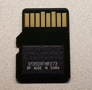
My card (and many of their higher-end cards – that is, not their Ultra lineup) features test pads that aren’t covered by solder mask, but are instead covered by some sort of screen-printed epoxy with a laser-etched serial number on top. With a bit of heat and some scraping, I was able to remove the (very brittle) coating on top of the test pads; this also removed the serial number which I believe is an anti-tamper measure by SanDisk.
-
- Epoxy coating over test pads
-

- Test pads exposed
After cleaning off any last traces of the epoxy coating, I was greeted with the familiar SanDisk test pad layout, plus a few extra on the bottom.
Building the Breakout Board
The breakout board is relatively simple in concept: for each test pad, bring out a wire that goes to a bigger test point for easier access, and wire up the normal SD bus to an SD connector to let the controller do its work with twiddling the NAND Flash bus. Given how small each test pad is (and how many), things get a bit… messy.
-
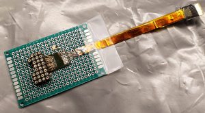
- Breakout board assembled.
-
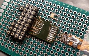
- Closeup of card breakout.
I started by using double-side foam adhesive tape to secure the SD card to a piece of perfboard. I then tinned all of the pads and soldered a small 1uF ceramic capacitor across the card’s power (Vcc) and ground (GND) test pads. Using 40-gauge (0.1 mm, or 4-thousandths of an inch!) magnet wire, I mapped each test pad to its corresponding machine-pin socket on the perfboard. Including the extra test pads, that’s a total of 28 tiny wires!
For the SD connector side of things, I used a flex cable for the XTC 2 Clip (a tool used to service HTC Android devices), as it acted as a flexible “remote SD card” and broke out the signals to a small ribbon cable. I encased the flex cable with copper tape to act as a shield against electrical noise and to provide physical reinforcement, and soldered the tape to the outer pads on the perfboard for reinforcement. The ribbon cable end was then tinned and each SD card’s pin was wired up with magnet wire. The power lines were then broken out to an LED and resistor to indicate when the card was receiving power.
Bus Analysis
With all of the test pads broken out to an array of test pins, it was time to make sense of what pins are responsible for accessing the NAND Flash inside the card.
Test Pad Pinout
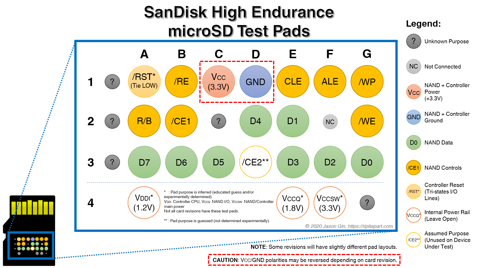
Diagram of the test pads on SanDisk’s High Endurance microSD card. (click to enlarge)
The overall test pad pinout was the same for other microSD cards from SanDisk, but there were some differences, primarily regarding the layout of the power pads; notably, the main power pins are backwards! This can destroy the card if you’re not careful when applying power.
CORRECTION (July 22, 2020): I might actually have just gotten my own documentation mixed up in terms of the power and ground test pads. Regardless, one should always be careful to ensure the correct power polarity is sent to a device.
I used my DSLogic Plus logic analyzer to analyze the signals on all of the pins. Since the data pinout was previously discovered, the hard part of figuring out what each line represented (data bus, control, address, command, write-protect, ready/busy status) was already done for me. However, not all of the lines were immediately evident as the pinouts I found online only included the bare minimum of lines to make the NAND Flash accessible, with one exception being a control line that places the controller into a reset state and releases its control of the data lines (this will be important later on).
By sniffing the data bus at the DSLogic’s maximum speed (and using its 32 MB onboard buffer RAM), I was able to get a clear snapshot of the commands being sent to the NAND Flash from the controller during initialization.
Bus Sniffing & NAND I/O 101 (writing commands, address, reading data)
In particular, I was looking for two commands: RESET (0xFF), and READ ID (0x90). When looking for a command sequence, it’s important to know how and when the data and control lines change. I will try to explain it step-by-step, but if you’re interested there is an introductory white paper by Micron that explains all of the fundamentals of NAND Flash with much more information about how NAND Flash works.
-

- Logic analyzer trace of RESET command. Dotted line indicates where the write and reset occurs.
-

- Logic analyzer trace of READ ID command. Dotted lines indicate where read/writes occur.
When a RESET command is sent to the NAND Flash, first the /CE (Chip Select, Active Low) line is pulled low. Then the CLE (Command Latch Enable) line is pulled high; the data bus is set to its intended value of 0xFF (all binary ones); then the /WE (Write Enable, Active Low) line is pulsed from high to low, then back to high again (the data bus’ contents are committed to the chip when the /WE line goes from low to high, known as a “rising edge”); the CLE line is pulled back low to return to its normal state. The Flash chip will then pull its R/B (Ready/Busy Status) line low to indicate it is busy resetting itself, then releases the line back to its high state when it’s finished.
The READ ID command works similarly, except after writing the command with 0x90 (binary 1001 0000) on the data bus, it then pulls the ALE (Address Latch Enable) line high instead of CLE, and writes 0x00 (all binary zeroes) by pulsing the /WE line low. The chip transfers its internally programmed NAND Flash ID into its internal read register, and the data is read out from the device on each rising edge of the /RE (Read Enable, Active Low) line; for most devices this is 4 to 8 bytes of data.
NAND Flash ID
For each NAND Flash device, it has a (mostly) unique ID that identifies the manufacturer, and other functional data that is defined by that manufacturer; in other words, only the manufacturer ID, assigned by the JEDEC Technology Association, is well-defined.
The first byte represents the Flash manufacturer, and the rest (2 to 6 bytes) define the device’s characteristics, as set out by the manufacturer themselves. Most NAND vendors are very tight-lipped when it comes to datasheets, and SanDisk (and by extension, Toshiba/Kioxia) maintain very strict control, save for some slightly outdated leaked Toshiba datasheets. Because the two aforementioned companies share their NAND fabrication facilities, we can reasonably presume the data structures in the vendor-defined bytes can be referenced against each other.
In the case of the SanDisk High Endurance 128GB card, it has a NAND Flash ID of 0x45 48 9A B3 7E 72 0D 0E. Some of these values can be compared against a Toshiba datasheet:
| Byte Value (Hex) | Description/Interpretation |
|---|---|
| 45 |
|
| 48 |
|
| 9A |
|
| B3 |
|
| 7E |
|
| 72 |
|
| 0D |
|
| 0E |
|
Although not all byte values could be conclusively determined, I was able to determine that the SanDisk High Endurance cards use BiCS3 3D TLC NAND Flash, but at least it is 3D NAND which improves endurance dramatically compared to traditional/planar NAND. Unfortunately, from this information alone, I cannot determine whether the card’s controller takes advantage of any SLC caching mechanisms for write operations.
The chip’s process geometry was determined by looking up the first four bytes of the Flash ID, and cross-referencing it to a line from a configuration file in Silicon Motion’s mass production tools for their SM3271 USB Flash drive controller, and their SM2258XT DRAM-less SSD controller. These tools revealed supposed part numbers of SDTNAIAMA-256G and SDUNBIEMM-32G respectively, but I don’t think this is accurate for the specific Flash configuration in this card.
External Control
I wanted to make sure that I was getting the correct ID from the NAND Flash, so I rigged up a Texas Instruments MSP430FR2433 development board and wrote some (very) rudimentary code to send the required RESET and READ ID commands, and attempt to extract any extra data from the chip’s hidden JEDEC Parameter Page along the way.
My first roadblock was that the MSP430 would reset every time it attempted to send the RESET command, suggesting that too much current was being drawn from the MSP430 board’s limited power supply. This can occur during bus contention, where two devices “fight” each other when trying to set a certain digital line both high and low at the same time. I was unsure what was going on, since publicly-available information didn’t mention how to disable the card’s built-in controller (doing so would cause it to tri-state the lines, effectively “letting go” of the NAND bus and allowing another device to take control).
I figured out that the A1 test pad (see diagram) was the controller’s reset line (pulsing this line low while the card was running forced my card reader to power-cycle it), and by holding the line low, the controller would release its control of the NAND Flash bus entirely. After this, my microcontroller code was able to read the Flash ID correctly and consistently.

Reading out the card’s Flash ID with my own microcontroller code.
JEDEC Parameter Page… or at least what SanDisk made of it!
The JEDEC Parameter Page, if present, contains detailed information on a Flash chip’s characteristics with far greater detail than the NAND Flash ID – and it’s well-standardized so parsing it would be far easier. However, it turns out that SanDisk decided to ignore the standard format, and decided to use their own proprietary Parameter Page format! Normally the page starts with the ASCII string “JEDEC”, but I got a repeating string of “SNDK” (corresponding with their stock symbol) with other data that didn’t correspond to anything like the JEDEC specification! Oh well, it was worth a try.
I collected the data with the same Arduino sketch as shown above, and pulled 1,536 bytes’ worth of data; I wrote a quick program on Ideone to provide a nicely-formatted hex dump of the first 512 bytes of the Parameter Page data:
Offset 00:01:02:03:04:05:06:07:08:09:0A:0B:0C:0D:0E:0F 0123456789ABCDEF
------ --+--+--+--+--+--+--+--+--+--+--+--+--+--+--+-- ----------------
0x0000 53 4E 44 4B 53 4E 44 4B 53 4E 44 4B 53 4E 44 4B SNDKSNDKSNDKSNDK
0x0010 53 4E 44 4B 53 4E 44 4B 53 4E 44 4B 53 4E 44 4B SNDKSNDKSNDKSNDK
0x0020 08 08 00 08 06 20 00 02 01 48 9A B3 00 05 08 41 ..... ...H.....A
0x0030 48 63 6A 08 08 00 08 06 20 00 02 01 48 9A B3 00 Hcj..... ...H...
0x0040 05 08 41 48 63 6A 08 08 00 08 06 20 00 02 01 48 ..AHcj..... ...H
0x0050 9A B3 00 05 08 41 48 63 6A 08 08 00 08 06 20 00 .....AHcj..... .
0x0060 02 01 48 9A B3 00 05 08 41 48 63 6A 08 08 00 08 ..H.....AHcj....
0x0070 06 20 00 02 01 48 9A B3 00 05 08 41 48 63 6A 08 . ...H.....AHcj.
0x0080 08 00 08 06 20 00 02 01 48 9A B3 00 05 08 41 48 .... ...H.....AH
0x0090 63 6A 08 08 00 08 06 20 00 02 01 48 9A B3 00 05 cj..... ...H....
0x00A0 08 41 48 63 6A 08 08 00 08 06 20 00 02 01 48 9A .AHcj..... ...H.
0x00B0 B3 00 05 08 41 48 63 6A 08 08 00 08 06 20 00 02 ....AHcj..... ..
0x00C0 01 48 9A B3 00 05 08 41 48 63 6A 08 08 00 08 06 .H.....AHcj.....
0x00D0 20 00 02 01 48 9A B3 00 05 08 41 48 63 6A 08 08  ...H.....AHcj..
0x00E0 00 08 06 20 00 02 01 48 9A B3 00 05 08 41 48 63 ... ...H.....AHc
0x00F0 6A 08 08 00 08 06 20 00 02 01 48 9A B3 00 05 08 j..... ...H.....
0x0100 41 48 63 6A 08 08 00 08 06 20 00 02 01 48 9A B3 AHcj..... ...H..
0x0110 00 05 08 41 48 63 6A 08 08 00 08 06 20 00 02 01 ...AHcj..... ...
0x0120 48 9A B3 00 05 08 41 48 63 6A 08 08 00 08 06 20 H.....AHcj.....
0x0130 00 02 01 48 9A B3 00 05 08 41 48 63 6A 08 08 00 ...H.....AHcj...
0x0140 08 06 20 00 02 01 48 9A B3 00 05 08 41 48 63 6A .. ...H.....AHcj
0x0150 08 08 00 08 06 20 00 02 01 48 9A B3 00 05 08 41 ..... ...H.....A
0x0160 48 63 6A 08 08 00 08 06 20 00 02 01 48 9A B3 00 Hcj..... ...H...
0x0170 05 08 41 48 63 6A 08 08 00 08 06 20 00 02 01 48 ..AHcj..... ...H
0x0180 9A B3 00 05 08 41 48 63 6A 08 08 00 08 06 20 00 .....AHcj..... .
0x0190 02 01 48 9A B3 00 05 08 41 48 63 6A 08 08 00 08 ..H.....AHcj....
0x01A0 06 20 00 02 01 48 9A B3 00 05 08 41 48 63 6A 08 . ...H.....AHcj.
0x01B0 08 00 08 06 20 00 02 01 48 9A B3 00 05 08 41 48 .... ...H.....AH
0x01C0 63 6A 08 08 00 08 06 20 00 02 01 48 9A B3 00 05 cj..... ...H....
0x01D0 08 41 48 63 6A 08 08 00 08 06 20 00 02 01 48 9A .AHcj..... ...H.
0x01E0 B3 00 05 08 41 48 63 6A 08 08 00 08 06 20 00 02 ....AHcj..... ..
0x01F0 01 48 9A B3 00 05 08 41 48 63 6A 08 08 00 08 06 .H.....AHcj.....
Further analysis with my DSLogic showed that the controller itself requests a total of 4,128 bytes (4 kiB + 32 bytes) of Parameter Page data, which is filled with the same repeating data as shown above.
Reset Quirks
When looking at the logic analyzer data, I noticed that the controller sends the READ ID command twice, but the first time it does so without resetting the Flash (which should normally be done as soon as the chip is powered up!). The data that the Flash returned was… strange to say the least.
| Byte Value (Hex) | Interpreted Value |
|---|---|
| 98 |
|
| 00 |
|
| 90 |
|
| 93 |
|
| 76 |
|
| 72 |
|
This confused me initially when I was trying to find the ID from the logic capture alone; after talking to a contact who has experience in NAND Flash data recovery, they said this is expected for SanDisk devices, which make liberal use of vendor-proprietary commands and data structures. If the fourth byte is to be believed, it says the block size is 4 megabytes, which I think is plausible for a modern Flash device. The rest of the information doesn’t really make any sense to me apart from the first byte indicating the chip is made by Toshiba.
Conclusion
I shouldn’t have to go this far in hardware reverse-engineering to just ask a simple question of what Flash SanDisk used in their high-endurance card. You’d think they would be proud to say they use 3D NAND for higher endurance and reliability, but I guess not!
Downloads
For those that are interested, I’ve included the logic captures of the card’s activity shortly after power-up. I’ve also included the (very crude) Arduino sketch that I used to read the NAND ID and Parameter Page data manually:

Pingback: Unboxing and review of SanDisk 64GB microSDXC High Endurance Card | Rip It Apart – Jason's electronics blog-thingy
my takeaway from reading available datasheets (and the differences between models listed) was that high endurance with the SD cards is in no way about write endurance (TBW), but only about the environment. So higher temperature ranges first of all.
LikeLike
Interesting, thanks for the insight. I also find it interesting that for applications like SBCs (Raspberry Pi, etc.), I’ve seen them denounce their regular Ultra lineup of cards in those too, and they point to the High Endurance lineup.
LikeLike
Out of curiosity, what kind of flex ribbon cable is that in the picture with caption “Breakout board assembled.” ?
LikeLike
They are flex cables for the XTC 2 Clip, albeit covered in copper tape. I bought mine about 4 years ago but the eBay listing is still active:
https://www.ebay.com/itm/401157144150
LikeLike
What pulsing time frame you use on A1 pad and how you know when start holding the line low.
LikeLike
I didn’t measure the timing as I just manually bridged a wire from A1 to ground. It was a simple tap of the wire that was enough for the card reader to issue a reset afterwards.
LikeLike
Very cool, nice work. Would it be reasonable then to assume that their Max Endurance series (SDSQQVR) is essentialy the same but with MLC 3D NAND? Assuming their “Hours of Full HD Recording”-to-TBW conversion is the same for both, they spec about a 6x improvement in endurance.
LikeLike
That would make sense. I might get a Max Endurance card to analyze for myself.
(EDIT: I just purchased a 128GB model of the MAX Endurance card for analysis!)
LikeLike
Update: I’m reverse-engineering the NAND inside the MAX Endurance lineup, and they’re using the same 3D TLC NAND as in the High Endurance, but in pMLC (pseudo-MLC) mode, so they’re using 2 out of the 3 bits per cell.
Blog post to follow.
LikeLike
Pingback: Ramble: 2020 in review | Rip It Apart – Jason's electronics blog-thingy
Hi! Very good post! I’m searching for the best microsdxc card for write intensive jobs. What’s your opinion about SanDisk High Endurance, Extreme or Ultra, wich one will you choose?
LikeLike
For the best write endurance, I’d recommend the SanDisk MAX Endurance; it uses 3D pMLC NAND Flash (same 3D TLC as in the High Endurance, but using only 2 bits per cell). I’m still working on the writeup for that card, but SanDisk specifies a ~6x higher endurance figure compared to the High Endurance.
Otherwise, the High Endurance is the best fit for the job. I haven’t analyzed what’s in the Ultra or Extreme, but I imagine it’s the same Flash but not specified (or warranted) for write-intensive workloads.
LikeLike
Hello, could you meanwhile find out what the Flash looks like on the SanDisk Extreme Pro 64 gb? So far I couldn’t find anything on the internet. but my guess and online video compared show but this performs better, but this has nothing to do with the live time.
LikeLike
Totally agree as information on this topic are rare and most of the tests only focuse on performance instead of reliability.
I suppose performance no longer matters when you SD card is corrupted…
My own usage being most for OS installation purpose, several of my cards failed and had to be replaced (sometime only after a few months).
This make me think these cards are not really suitable for OS or write intensive application and I’m quite surprised not to see more talk on this subject..
Even if I could replace my failing card for free thanks to long warranty, you still loose your data and the time to reinstall the system.
So far I only had sandisk cards, would getting Samsung ones a better choice for this purpose?
Notably regarding their pro endurance line, is it worth the money for reliability or mainly marketing?
LikeLike
I don’t have a large selection of Samsung cards to test, but I believe the PRO Endurance line from Samsung does use proper MLC Flash. When you refer to your cards being corrupted, you’re referring to the specific SanDisk High Endurance cards, correct?
I’d imagine the Samsung ones to be pretty reliable, as they are fully-integrated as a manufacturer and continue to make excellent SSD products.
LikeLike
Nope it wasn’t endurance (never tried them actually as I thought it was for weather extreme condition only).
The most absurd failure happened on a 200 GB Sandisk Extra, that lasted about 2 months on desktop linux usage… which is kind of funny considering the 10 years warranty.
Another notable fail was with an SSD (but this time Samsung)… luckily 1 month before expiration of warranty (out of 5 years) so I got a new upgraded one for free..
Will follow your advice and try samsung PRO endurance next time.
Also just to mention it; a workaround to increase SD lifetime for OS purpose, is using read only system partition installation.
However this isn’t the most convenient solution.
LikeLike
Thank you for a very interesting article.
Also using Samsung Pro Endurance card as a pMLC which using 3D TLC?
It shows a runtime similar to Max Endurance.
There is information that Sammy is still producing 3D MLC NAND Flash.
I would be grateful if you could look it up even when you have the opportunity.
LikeLike
Using the Linux mmc-utils, you can read the manufacturer ID, CSD, CID, SCR, speed and power classes, extended CSD, write protect status, … Very helpful!
LikeLike
I suspect one reason why Sandisk isn’t willing to say much about what they use in the cards is because they’re not going to guarantee it. They’ll change these in the future depending on cost, availability etc. Saying it contains X is a good way to get sued when you change it.
LikeLike
I hate when they don’t post cycles(long standing trend) but you can easily see what it is based on recording hours, looking at their documentation it is based on 1080P recording which is ~149 MB/min. Now they conflated 64gb ENDURANCE WITH 128gb RECORDING ENDURANCE IN THEIR EMAIL… see- https://documents.westerndigital.com/content/dam/doc-library/en_us/assets/public/sandisk/product/memory-cards/high-endurance-uhs-i-microsd/data-sheet-high-endurance-uhs-i-microsd.pdf
64GB is only rated to 5,000 hours, 128GB gets 10000 hours. The math works out to 700 cycles regardless of capacity(or 0.96 DWPD over the 2 year warranty).
If you know the cycles, you have a pretty good certainty of guessing flash cell bit-density, and this is clearly TLC NAND cells. Range write cycles based on cell bit density below
SLC :10k-100k
MLC:1.5k-10k
TLC:600-2k+
QLC:150-600(Enterprise pushing 1500)
NAND controllers are still innovating and manufacturing processes maturing, lower bounds are pretty much set for what anyone is willing to release, the higher end is squeaking out more performance. I would think PLC will be the standard consumer medium in another couple years. Could easily see them moving from TLC to QLC as soon as the nand controller and flash media become capable of approaching the 700 cycles (business ROI calc, how many consumers are going to use all cycles within warranty term…)
LikeLike
Thanks!
I also found a post of somebody who wrote a sector of a SanDisk SD card 1.1 million times without problems (due to wear leveling). Also interesting. https://electronics.stackexchange.com/questions/420469/microsd-card-how-many-times-can-i-write-the-same-sector
LikeLike
Hello, I am very happy to read this paper of yours. This is a high quality blog. I like it very much.
I have a question to ask you.
If I don’t know the NAND ID, using the 90H command, how can I determine the sort order of IO/07–IO/01. —– 90h/00h READ ID
Only after knowing the NAND ID can you use the 90H command to arrange the order of IO/07–IO/01. —- 90h/00h READ ID
Of course, Intel, Micron, have INFO instructions that can be used. —– 90h/20h READ ID
90/20 READ ID command. This command returns an “ONFI” text string.
I think we can discuss NAND related issues together.
I can pay you if you help me with my NAND questions.
Thank you,
LikeLike
If you don’t already have the pinout to determine the pin ordering for the I/O[0..7] lines, you may have to do so by trial and error, which can be a lot more difficult if you don’t have a working device to sniff the data lines first. I don’t know of any other method to figure out how the data lines are ordered.
LikeLike
HELLO FOR ALL GENTELMANS
i want to add , that sandisk max endurance is for the moment perfect choice , also kioxia exceria
for best price quality !
western digital actualy it makes sandisk cards ,
there is also industrial cards with SLC but sure they are very expensive Mfactors.com you can find here https://mfactors.com/industrial-micro-sd/
about old sandisk extreme pro , before they seems to make them and apear more strong as material compare to new generation of extreme pro wich seems to be so poor in quality if you thinking to broke them or scratch
also apacer make industrial micro sd and you can find more info here
Click to access ak6-112jha-00103.pdf
here you can find out more specs about long life western digital cards
Click to access product-brief-western-digital-industrial-sd-microsd.pdf
and i guess best price quality is purple
Click to access en_prosi_wd-purple-microsd.pdf
it have also monitor to see lifetime used and left…
and up to Up to 768 TBW of data
king regards guys
LikeLike
Hi!
When will you review/reverse engineer/determine what kind of NAND flash does the Samsung PRO Endurance card has?
Here is a calculation:https://forums.wyzecam.com/t/bytes-bits-bitrates-fps-codecs-compression-and-samsung-pro-endurance-microsd-cards/17522/2
Also, Samsung is proven to lying and misleading people by saying MLC = TLC.https://dashcamtalk.com/forum/threads/microsd-options-including-mlc-cards.26035/page-13#post-468314
Also, SanDisk Max Endurance has longer warranty and claims more video recording hours.
In conclusion, I guess Samsung PRO Endurance has just 3D TLC NAND.
LikeLike
I haven’t decided yet, mainly because I haven’t really wanted to spend money on such a card that probably wouldn’t see much use myself.
LikeLike
There’s another interesting thing.
A few days ago I noticed that Samsung released a new version of their PRO Endurance card.
https://news.samsung.com/global/samsung-unveils-new-pro-endurance-memory-card-optimized-for-surveillance-and-dashboard-cameras
As you can see, the new Samsung PRO Endurance 32GB and 64GB cards have only V10 and U1 rating, while 128GB and 256GB versions have V30 and U3 rating. This means these new cards have inconsistent quality and performance (maybe different NAND).
Conversely, all Sandisk Max Endurance cards have V30 and U3 rating,
LikeLike
That’s certainly suspicious on Samsung’s part. I’d love to test the smaller and larger capacity cards, but the cost of obtaining the cards makes it financially unattractive for me to do so at this time.
LikeLike
Does the SanDisk High Endurance SD Cards have any kind of wear leveling management? I’m using it for the Windows 10 install on Steam Deck, if it knows how to spread out the wear I think it’ll be fine.
LikeLike
Yes, as all NAND-based storage devices use wear leveling. There are different kinds of wear leveling algorithms but the controllers in modern devices are smart enough to use more sophisticated algorithms to evenly distribute the workload across the NAND cells.
LikeLike
Pingback: 适合树莓派/SBC的MLC长寿命sd卡?SanDisk Max Endurance 32G tf卡简单测试 - WuSiYu Blog
Interesting! Did you check if the block size is indeed 12 MiB (768 pages)? I tested a Extreme PRO 128 GB using FlashBench and got a putative erase block size of 4 MiB.
(FlashBench: https://git.linaro.org/people/arnd/flashbench.git/; also available in Debian/Ubuntu/RaspiOS repos: apt install flashbench).
LikeLike
I didn’t. The SD card controller and its Flash management might introduce inaccuracies when testing, although I can’t confirm or refute my hypothesis at this time. Modern Flash storage technology is complex enough that the controller has to do a lot of behind-the-scenes work that is transparent to the host system.
4MB could make sense since that’s 1/3 of 12 MB, when addressing one of the three “levels” in TLC NAND Flash.
LikeLike
Interestingly, the tool can produce plots of read access times for a series of segments. An old article from the developer presents a sample plot produced with a “Panasonic Class 10 SDHC card” (see https://lwn.net/Articles/428584/). This plot shows two slightly different access times for certain segments. This might represent slightly slower and faster pages or the 2 “levels” of the MLC NAND flash. I did not yet create a plot for my SD card, which probably uses TLC flash …but it would be great if one could detect the number of “levels” this way…
Have a nice Sunday!
LikeLike
Just a question of a beginner.
You write: “4MB could make sense since that’s 1/3 of 12 MB, when addressing one of the three “levels” in TLC NAND Flash.”
Does this mean that one should align partitions to 12 MiB on TLC SD-cards with 4 MiB erase blocks? …or are there other parameters that should be set when formatting the SD card (e.g. alter stride, stripe-width in ext4).
LikeLike