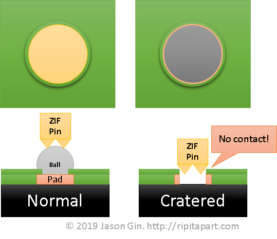
cratered bga diagram Published January 22, 2019 at 569 × 491 in eMMC Adventures, Episode 4: Recovering data from physically damaged BGA eMMC Flash storage chips Top and side diagram of normal and cratered BGA pad, with ZIF socket
