As seen on Hackaday!
TL;DR: The Atomic Pi single-board computer CAN be expanded through PCIe. It’s just a massive pain to do so, even if you have steady hands. Let’s just say it’s a long story…
DISCLAIMER: The modification performed in this blog post can, and has, caused permanent hardware damage to my Atomic Pi, albeit repairable with much skill and effort. Reenacting what I’ve done requires significant experience with SMT (surface-mount technology) components, some barely larger than a grain of sand (I consider 0402-size components to be “oversize” in this instance). I accept no responsibility for damages arising from attempting this modification.
Introduction
Single-board computers (SBCs) are all the rage nowadays, with the Raspberry Pi being the most well-known in this category. SBCs are compact computers, carrying their own CPU and memory, and usually some on-board storage and various I/O connections (e.g. USB, HDMI, Ethernet). Most of these computers use the ARM architecture, found on almost all mobile devices today. However, some use the x86 architecture, which is used in higher-end tablets, laptops and desktop computers.
Recently, the Atomic Pi made waves in the electronics hobbyist space, boasting an Intel Atom Z8350 quad-core CPU with 2 GB of RAM, 16GB of eMMC storage, Gigabit Ethernet, Wi-Fi, USB 3.0, built-in speaker amplifiers, and lots of general-purpose I/O (GPIO) pins – all for less than $40 USD!
-

-
An (unmodified) Atomic Pi SBC.
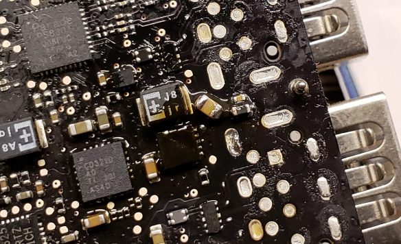
As one might expect, there were caveats to this little computer, with some dismissing it very harshly, if not unfairly. With some investigative work, members of the community found out that the “Atomic Pi” board actually belonged to the Kuri robot from Mayfield Robotics; the company shut down in late 2018, and the liquidated stock of these SBCs were snatched up by Digital Loggers with the help of a Kickstarter campaign, who then developed breakout boards to make using them easier. This is because – unlike almost every other SBC – you can’t just plug in a barrel jack or USB cord to power it! Instead, it uses a 2×13 pin header, which many users did not have on hand, nor had the skill and/or resources to build their own solution. This is compounded by the board’s need for clean, well-regulated 5 volts at 2-4 amps, with 12 volts being optional to power the onboard speaker amplifier. The 16 gigabytes of eMMC storage proved to be too cramped to run Windows 10 directly, and the Realtek RTL8111G Gigabit Ethernet chipset is often frowned upon by those in the pfSense (a free firewall/router OS) community.
-

-
My own DC input board for the Atomic Pi. 12-volt barrel jack input is converted to 5 volts with a DC-DC converter module.
The NIC’s usage of the Z8350’s single PCI Express (PCIe) lane is what caught my attention. Unfortunately, the RTL8111G Ethernet chip is soldered to the board, with no easy method to replace it with an external card. A few people have attempted to remove the chip and wire in an external PCIe riser, without success. With my previous experience with fine-pitch electronics work, I figured that this would be a fairly easy modification to make.
It wasn’t. In fact, this was one of the most frustrating electronics projects I’ve done to date – and now you get to come with me in my adventures (and misadventures) in microsoldering on the Atomic Pi (or was it Kuri? The jury seems to be out on the nomenclature).
Optional Reading: PCI Express Signals
PCI Express (or PCIe for short) is a very common high-speed interface for connecting processors or chipsets to all sorts of different peripherals. It uses low-voltage differential signaling to minimize interference, and a single lane of PCIe can carry 250 MB/s for the first generation, all the way up to 2 GB/s for the fourth generation!
A single PCIe lane is made up of three differential pairs: receive, transmit, and a 100 MHz reference clock. Control signals for waking up and resetting peripherals are also provided. Riser cards, often used for cryptocurrency mining, use these five signals to provide the minimum connectivity for any PCIe peripheral. The interface is highly flexible, allowing graphics cards that normally use 16 lanes to run on just one lane. The specifications for PCIe make board design easier, as the differential lines are designed to adapt to different lane configurations; the polarities in a pair (transmit, receive, clock) are polarity independent (all that matters is that you maintain a good differential pair).
PCIe Signal Pinout
Since the Atomic Pi lacks a PCIe slot of any kind, I have provided the diagram indicating which signals go to what points on the board:
-

-
PCIe signal diagram, indicating which signals are required.
Note that the AC coupling capacitors are required for the peripheral Rx (receive) pair, and are optional for the peripheral Tx (transmit) pair.
Attempt 1: “Chipple” Bypass
I started this project with the intent of making my modifications as reversible as possible. Looking at the RTL8111E’s datasheet (a similar model to the 8111G) revealed the presence of an “ISOLATEB” pin; grounding this pin causes the chip to disable itself and release its hold on the PCI Express lines.
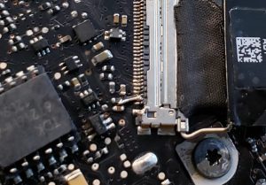
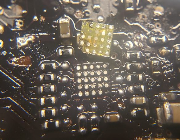
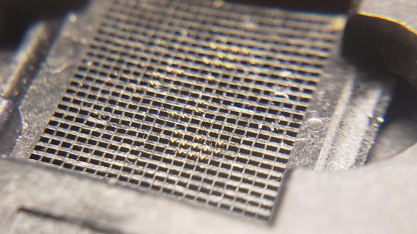
This brings us to the first roadblock: the Ethernet chip is soldered to the board, and the components that connect it are known as 0201 (0.002 inches in length, 0.001 inches in width), smaller than a breadcrumb!
After disabling the Ethernet chip, I used my trusty 0.1mm (that’s four-thousandths of an inch!) magnet wire to tap into the PCIe lines, and brought them out to a PCIe riser card, which provided a USB 3.0-type socket for an external connection.
-

-
First attempt to get external PCIe on the Atomic Pi, using magnet wire. White wire ties ISOLATEB low, disabling the Ethernet chip.
Unfortunately, high-speed signals aren’t just about wiring from one device to the next, and this was no exception. The rat’s nest of wires were no suitable medium for the 5-gigabit signals to traverse (PCIe requires very tight control of electrical trace layouts), and the Atomic Pi was unable to detect the presence of any device on the external PCIe port.
Attempt 2: Thin Twinax Troubles
With the signaling issue in mind, I tried some very thin twinaxial cables from a dead MacBook’s hard drive cable to connect the PCIe lines to my riser card. This cable is very thin, with an outer thickness similar to fishing line. It uses a foil and wire “shield” around the two internal wires to protect it from external interference. I figured that this should help protect the delicate signals from the harsh outside world.
I didn’t have very much of this thin twinax cable on hand (that said, if anyone knows where I can buy this stuff in bulk, please let me know!), so I was limited to very short lengths for each pair. I ran out of twinax after the transmit and receive pairs, and resorted to using two coaxial cables from that same cable bundle.
-

-
Preparing for the second attempt. Thin twinax soldered to the AC coupling capacitors.
-

-
Second attempt to break out PCIe to the riser, using thin twinaxial cable.
After fiddling with the super-thin wires and soldering them to the header, I still got nowhere and could not get the Atomic Pi to see an external PCIe card.
Removing my modifications revealed my first blunder: despite placing the chip into a temporarily disabled state, the Ethernet chip was dead! This meant that I could not use the built-in Ethernet port anymore, and the LEDs next to the Ethernet port simply glowed a dull orange instead of their rapid blinking pattern when data is being transmitted over Ethernet. I figured that there was no use keeping the chip on the board, so I used my hot air rework station to remove it, using a generous amount of heat and flux to get the chip removed.
Attempt 3: To Ribbons, You Say?
With the dead Ethernet chip removed, I decided to use another tactic to bring out the PCIe interface. I decided to use a thin ribbon cable (okay, more accurately a “flat flexible cable”) to help decouple any mechanical stresses from moving the external USB 3.0 connector around during testing, and its compact size allowed me to try using the QFN pads to connect my ribbon cable, hopefully minimizing noise that could be picked up, as well as avoiding any “stubs” of wiring within the differential pair that would degrade the signals.
The challenge is that the chip uses a very small pad spacing, and I wanted to avoid soldering directly to the ribbon cable. I managed to salvage a couple connectors from some other devices, and used a cut-up CompactFlash memory card’s PCB to make it easier to solder the connector, as well as provide a base for the connector to sit on.
-

-
Third attempt using ribbon cable connector on miniature PCB for connection to the QFN footprint.
-

-
The other not-so-elegant end to the ribbon cable.
-

-
Ribbon cable with foil shielding tape, as used on HP eMMC module.
The connector on the board was affixed onto the Ethernet chip’s footprint with the help of some double-sided foam tape, and magnet wire was used to bond the PCIe signal wires onto the ribbon cable. The ribbon itself used copper foil on one side to help with interference suppression, and provide the signals a “ground plane” to travel across.
Things weren’t quite as elegant on the other end of the cable, however. I still had to contend with a fine-pitch ribbon connector, and a way to connect that to a male USB 3.0 plug to hook it up to the PCIe riser. I had little option except to use the small lengths of twinax from the last attempt, and (perhaps unsurprisingly) it didn’t work.
Attempt 4: Teeny Tiny Twists
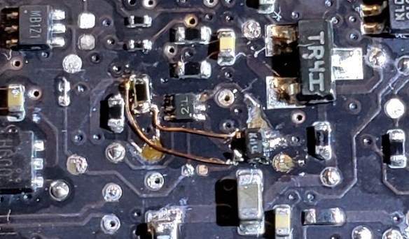
The next attempt went to a smaller scale, using a very fine twisted pair I created out of my 40 AWG magnet wire (each wire is as thick as a hair). I then shielded this magnet wire by sandwiching it between pieces of copper tape to act as a ground plane for the signals. I reused a dead USB 3.0 drive to act as the plug for the PCIe riser, and wired it straight to the QFN pads of the original Ethernet chip.
-

-
Fourth attempt, using handmade twisted pair.
-

-
Super-tiny twisted pair hooked up to dead USB 3.0 drive PCB.
Although the twisted pair would have, in theory, reduced intra-pair skew and some degree of EMI resistance thanks to the copper tape, the homemade twisted pair almost certainly would not have provided a 100-ohm differential impedance that’s required for PCIe signaling. Once again, the attempt to break out PCIe from the Atomic Pi was a failure.
Attempt 5: SASsiness Yields Results…?
Since the central issue with external PCIe connectivity involved the connection between the Atomic Pi board and the riser, I figured I would try a medium that was specifically intended for high-speed differential signals. I bought some thin SATA cables (specifically the 18-inch thin cables on Amazon), which used two pairs of thin SAS cable per SATA connection. The difference between SATA, SAS and PCIe is of little difference here, as the key criteria was a differential pair with 100-ohm impedance and ability to carry high-frequency signals.
-

-
Internals of a SAS cable.
Despite being a thin cable (each conductor is only 30 AWG, or 0.25 mm in diameter), these cables were too stiff to directly connect to the AC coupling capacitors without a very high risk of damaging the capacitor and/or the pad it is soldered to. I had to reinforce the cables by soldering them down and hot gluing the cables to the board at multiple points to relieve stress on the connections.
-

-
Fifth attempt to get external PCIe, and finally got a connection!
-

-
Soldering straight to the PCIe riser connector.
-

-
PCIe connection successful… for now.
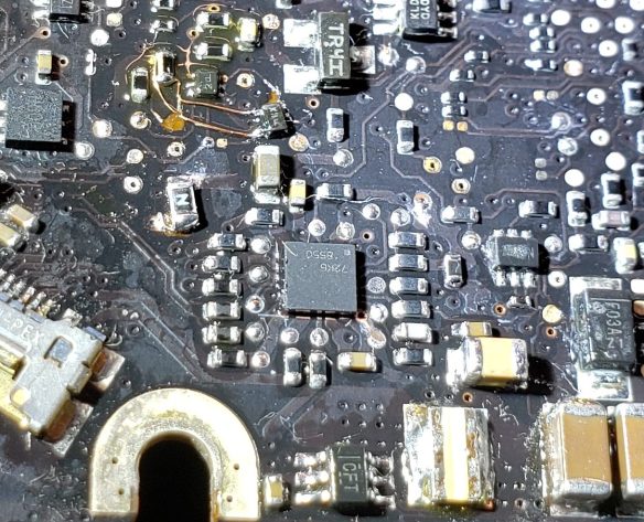
The original 0201-sized AC coupling capacitors were removed, and more reasonably-sized 0402 capacitors were used in their place. Each capacitor was a common 100nF capacitance, and were easy to harvest from some dead laptop motherboards I had on hand. I “flipped” the layout of the capacitors away from the QFN footprint, but this meant that only one side of the capacitor was actually anchored to the board; this made the capacitors very fragile and I often lost the terminations on the capacitors (thankfully they are plentiful in electronic devices like this).
To help minimize stress on the vulnerable capacitors, I used magnet wire as a flexible “bridge” between the capacitor and the SAS cable, and the cables were tied down to solder tab wire that I used as “bus bars” for a strong electrical ground as well as a tie-down point to take away most of the strain of the cable’s flexion. Despite negatively affecting signal integrity, I was able to get a sufficiently stable connection to perform some initial testing, and I succeeded! I was able to connect an Intel 82576-based dual-port network card to my external riser.
-

-
Test setup of pfSense using external PCIe.
However, this didn’t last long. The simple movement of the wires on the board when trying to connect different peripherals was enough to break the AC coupling capacitors, despite the use of my flexible terminations from the SAS cable to the capacitors. Replacing the damaged capacitors and redoing the magnet wire terminations failed to restore connectivity, so I desoldered all of the existing connections and started over.
Attempt 6: We Have Lift-Off! (that’s bad)
In an attempt to further improve signal integrity, I decided to take the bold move of eschewing the flexible terminations of magnet wire, and decided to directly solder the SAS cable’s wires to the capacitors, which are soldered to the PCIe pads on the Atomic Pi. I anticipated that physical stresses would damage the capacitors, so I opted to use longer lengths of SAS cable, and to hot-glue the cable to the board at regular intervals to minimize the amount of stress that gets coupled into the cable and capacitors. The 100 MHz reference clock continued to use magnet wire for connection as it was at a much lower frequency than the PCIe signals, and reduced the amount of physical crowding around the PCIe pads.
This leads me to my next issue. To help with structural integrity, I repositioned one of the SAS cables so that it would remain on the board before going to the PCIe riser connector, meaning it would be perpendicular to the other cables. This required me to strip extra foil shielding to jump over the existing capacitors, which increases the risk of physical stress on the capacitors, as well as reduced signal integrity. Additionally, I used a longer set of twinax cables, sacrificing two SATA cables to get most of the original 18 inches of length per cable.
-

-
Ouch… Lost a capacitor pad.
-

-
Welp, I found the pad. It cannot be attached back to the board, sadly.
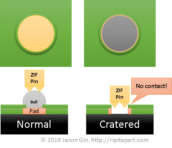
Testing of this construction method failed, and it was only at this point that I realized that two of the four AC coupling capacitors I used weren’t the same capacitance; PCIe usually uses 100 nF capacitors, but I had a 1 nF on one PCIe pair, and 10 nF on the other – no wonder things weren’t communicating (and that’s what I get for assuming the capacitors were the same)! Unfortunately, the process of removing the SAS cable connections resulted in the phenomenon I was trying to avoid: the board’s PERp0 (the positive side of the PCIe receiver) pad had lifted away from the PCB, leaving me with an unsolderable crater.
Attempt 7: Success!
After losing one of the pads for the original coupling capacitors, I was feeling pretty defeated. I didn’t let this stop me, and I decided to apply my magic skills with 40-gauge magnet wire to the trace, and was able to get a sufficient connection with a replacement 100 nF capacitor (and this time I measured it…), hopefully in such a way as to not too negatively affect signal integrity. Unfortunately, the 0201-sized resistors used to connect the PCIe reset and wake signals lost their terminations and no longer took solder on one end; I opted to keep the resistors in place and soldered magnet wire to the other end (facing the SoC rather than the Ethernet chip), as further measurement revealed that the resistors were simply 0-ohm jumpers anyway. I scrapped the longer SAS cables, and went back to the ~8-inch lengths to reduce attenuation.
-

-
Finally! Connections restored, circuit area prepared for epoxy sealant.
-

-
Reinforcement for the cables leaving the board.
-

-
Shortened PCIe cable end.
After rewiring the PCIe data, clock and control lines, I crossed my fingers and retried the riser with my Intel NIC – and it worked! After verifying the connections were sufficiently strong, I decided to make the modification permanent, and covered the area with epoxy to prevent any of the components from breaking loose. Additionally, I used some aluminum sheet metal, double-sided foam tape and some zip ties to create a reinforcement bar, helping to strengthen the cable connections as they leave the board.
With all the connections in place, it was time to get to the fun part: seeing what PCIe peripherals work on the Atomic Pi!
Testing Results
One interesting behaviour of the Atomic Pi when using Windows is that changing PCIe cards often causes the system to immediately power down or freeze during boot. Simply powering the board on again seems to fix this issue. Why am I using Windows? I already upgraded the board to a 64GB eMMC instead of the original 16GB, and the appeal of the Atomic Pi’s x86 architecture was the ability to run desktop apps – in particular, Windows apps.
The UEFI firmware has a hidden advanced menu, accessible if the “shutdown /r /fw” command is run as administrator. There is a section for PCIe settings, and the ones that interested me were the AER (Advanced Error Reporting) and PCIe hot-plug settings. Unfortunately, these do not seem to have any effect as Windows doesn’t seem to pick up any hardware events in the Event Log.
Test 1: Network Devices
PASS: Intel 82576 Dual-Port Adapter
-

-
Atomic Pi with Intel 82576 NIC, powered by Ethernet!
If the port(s) have a connection to another device (e.g. a network switch), the orange and green LEDs will illuminate soon after the PCIe link is properly initialized, which makes for quicker troubleshooting. Even if the system is off, the green link LED remains lit, but goes out once the PCIe bus is reset.
The card works a treat in pfSense and Windows, allowing high-performance Gigabit-speed transfers with both ports in use. However, the UEFI firmware does not recognize the card as a bootable medium (which is for the best in my opinion – the PXE boot program tends to hinder the boot process more than anything).
PASS: Realtek RTL8111GS (External Card)
The PXE network boot program built into the UEFI firmware works just fine, which is expected as the chip is the same type as the original RTL8111G, with the exception that the chip has a built-in switching converter rather than the linear LDO that the Atomic Pi uses natively.
PASS: JMicron JMC250
The card works in Windows and pfSense; the particular card I have has always been flaky in operation, and this was no exception.
PASS: ASUS PCE-N15 (Realtek RTL8192CE) 802.11n WLAN Adapter
Using this card is a performance downgrade compared to the dual-band adapter already present on the Atomic Pi, but it did function correctly in Windows.
Test 2: External Graphics Cards (eGPU)
PASS: EVGA/nVidia 8500 GT
The UEFI firmware doesn’t seem to want to acknowledge the presence of PCIe graphics adapters, which results in issues when testing in Windows. Initially, the card failed to enumerate correctly, identifying as a Microsoft Basic Display Adapter and displaying an error in Device Manager:
This device is not working properly because Windows cannot load the drivers required for this device. (Code 31)
The driver trying to start is not the same as the driver for the POSTed display adapter.
Manually downloading and installing the drivers allowed the card to work properly. As previously mentioned, the UEFI does not recognize the presence of the graphics card, so a monitor that is plugged into the graphics card won’t start working until Windows is loaded and the graphics driver initializes.
Additionally, the adapter’s resources won’t be used if the monitor is connected to the Atomic Pi’s built-in HDMI port – it’s a tradeoff between graphics performance and the ability to see what’s happening on boot; maybe this is different in a multi-monitor configuration, but I didn’t have enough desk space to test this.
PASS: XFX/AMD Radeon 4650
The same driver issues popped up when using this card as well, and the same fix applies.
PASS: ASUS/nVidia GTX 660 Ti
Ditto. This card was the best I had on hand for testing, and amusingly it consumes about 10-20 times the amount of power that the Atomic Pi uses, and is bigger in size as well.
-

-
External graphics card connected to the Atomic Pi. The card is bigger than the computer!
Connecting this card allowed me to run games that would otherwise simply not work, such as Just Cause 2. It performed at about 20-30 frames per second: not great but not terrible. Just Cause 3 was absolutely painful to run, but this is not surprising as the Atomic Pi’s hardware is far below the game’s minimum requirements in almost all aspects.
Test 3: Storage
PASS: Dell PERC H200 SAS Adapter
-

-
SAS bootable device entry in UEFI.
To my surprise, not only will it work in Windows, it even supports booting from the UEFI! It mentions a SAS controller driver during boot, but I am not sure as to whether this is present in the Atomic Pi’s UEFI, or if it is a driver provided by the SAS adapter itself. The PCIe 2.0 1x interface limits the maximum throughput to less than 500 MB/s, which is slower than a single SATA III connection, and informal testing showed a maximum speed of about 330 MB/s. I have not investigated whether I could configure the hardware RAID features of the adapter from the operating system, but I imagine that doing so would dramatically improve performance when running a RAID 1 (mirrored) setup.
FAIL: OWC (What’s This?) Aura Pro X 480GB NVMe SSD
This SSD was originally meant as an aftermarket SSD upgrade for a MacBook Air, but I bought a PCIe adapter card to use it in a regular PC. I was able to get it to enumerate in Windows, but any sort of read/write action caused it to lock up and throw errors in the Windows Event Log. I suspect this is likely a power supply issue due to how the PCIe riser board provides power (12 volts -> DC/DC converter -> 3.3V LDO linear regulator), or maybe the card just doesn’t want to cooperate.
FAIL: Marvell 88SE9128 2x SATA III + 1x PATA UDMA-133
This adapter caused Windows to almost freeze during boot. Instead, the boot animation would advance by one frame every 2 seconds until the card is removed. I suspect this is the PCIe bus attempting to negotiate a connection but failing, possibly due to signal integrity issues. Checking the Windows Event Log turned up nothing either.
Test 4: … More PCIe?
FAIL: Extender Cable
One would think that a simple straight-through cable would work, right? Nope – it seems like the signal has already been degraded enough after traveling across multiple non-ideal connections, and the extra length in a cable was just enough to degrade the signal beyond recovery.
PASS: PCIe Port Multiplier / ASMedia ASM1184e
UPDATE (July 3, 2019): It seems that the “USB 3.0” pinout on these PCIe risers is inconsistent. I was somehow able to make do by using a PCIe card plugged into my current riser, which then led to the ASM1184e board, which splits the PCIe 2.0 1x lane into four slots. It seems like the chip is able to handle the attenuation over such a long cable length, and it even includes a 100 MHz clock buffer, effectively “refreshing” the signal for more sensitive PCIe cards.
I tried the 88SE9128 card again, but still had no luck. Ethernet cards worked without issue, but I wasn’t able to test the graphics cards as the ASM1184e board’s PCIe slots are closed-ended 1x slots. I could try cutting the edge of the connector to allow for larger cards, but that’s an experiment for another day.
Conclusion
Despite all the roadblocks I encountered in this project (sometimes rage-inducing ones), I still enjoyed this project and the various techniques I tried along the way. The prospect of attaching desktop PCI Express peripherals to a CPU designed for a tablet opens up many different applications for the Atomic Pi, including ones that would otherwise have been less efficient or impossible using the board’s built-in hardware (e.g. dual Gigabit Ethernet without using USB, or GPU-intensive computing workloads).
The high-speed nature of modern computer systems presents many challenges for engineers and modders alike. Multi-gigabit interfaces easily reach into the realm of radio-frequency (RF) electronics, where things like AC transmission line effects and differential signal routing become very important. This issue, coupled with the fact that most modern devices use very small components, makes it difficult for many electronics hobbyists to access these interfaces on their own. Although a modification like what I did is technically possible, I don’t consider it practical for an average electronics/computer enthusiast.
Future Ideas
One avenue I’ve thought about pursuing is a mod board that is soldered onto the Atomic Pi’s PCB, allowing a more robust connection for the PCIe lines; this would include signal integrity improvements like ESD protection and PCIe line redrivers to strengthen the signals to/from the SoC and peripheral(s). PCB design is currently beyond my scope of knowledge, but it would be a fun way to dive right into the subject matter.