PPS For All: Directly charging lithium-ion batteries with a USB-C PD tester

TL;DR – USB-C with PPS (Programmable Power Supply) technology is here, it’s cool, and now it’s usable on more than just the newest smartphones – it works on almost any Li-ion battery with the right USB-C tester. Check out the GitHub repo – it’s open-source!

As seen on Hackaday!

DISCLAIMER: Lithium-ion batteries can be dangerous if mishandled or abused! While much testing and development has resulted in a fairly stable implementation, this application is still an “off-label” use of a USB PD charger and USB-C tester, and therefore there is a risk of property damage, personal injury, or other unforeseen consequences if something goes wrong (and I will NOT be held responsible for that!).

Introduction

The USB PD (Power Delivery) standard has revolutionized how we charge our everyday electronic devices. While many new devices (such as smartphones) emphasize “fast charge” capability, it has required changes to both the device itself, as well as the adapters that power them.

Because power losses in the charging cable (or any other resistance) is directly related to the amount of current flowing through it, one can get more power for the same amount of current by increasing the voltage (this is how the AC power transmission lines that you see on the street and countryside work as well). The USB PD standard allows a device to request the adapter to increase its output voltage from 5 volts to a higher level, such as 9, 15, or 20 (and sometimes 12) volts.

An addition in the third version of the USB PD standard added optional PPS (Programmable Power Supply) support for the power adapter, which allows an adapter to output a wide range of voltages, rather than a fixed “menu” of 5, 9, 15, 20 (and sometimes 12) volts.

What is USB-C PPS charging?

PPS charging is a relatively new variation to the existing PD charging scheme. It allows the device being charged to actively communicate with the adapter and request a precise voltage (and current) level, increasing efficiency since DC-DC conversion efficiency drops when the difference in voltage between the input (the adapter) and output (the battery) is larger. With this bidirectional communication, it allows the adapter to share some of the regulation workload, and therefore move some of the heat-generating power conversion to the adapter, allowing the device’s battery to charge at a cooler temperature which improves its lifespan.

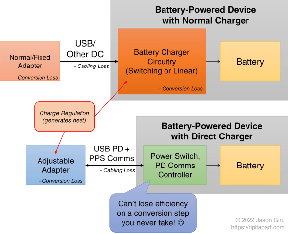
Direct Battery Charging

One step past normal PPS charging is direct charging, which completely offloads the power management to the adapter; the host device controls the charge process purely via software commands to the adapter. This is analogous to the DC fast charging method used in electric vehicles (EVs), which also perform all power regulation outside of the vehicle and its internal charge circuitry. Because the device no longer needs to perform its own DC-DC conversion, this skips a step in the power conversion “chain”, increasing efficiency and reducing the amount of heat dissipated in the host device (you can’t lose power on a conversion step if you never perform that step in the first place!). With this reduction in internally-generated heat, the battery can be charged at even faster rates than it could with previous charging schemes.

One barrier to the widespread adoption of direct charging is that it requires the device to explicitly support it, as it requires significant changes to how the “power path” is designed internally. It also requires the adapter to support the voltage and current levels required by the host.

Diagrams comparing normal versus direct charging schemes.

Diagrams comparing normal versus direct charging schemes. (click here for full-size image)

Thankfully, on the adapter side, PPS support is becoming more and more common, even though most devices on the market (at least at the time of writing) don’t support it. However, because that potential is already present, perhaps there’s a way for the electronics hobbyist to take advantage of direct charging for their own batteries…

Shizuku Platform and its Lua API

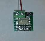
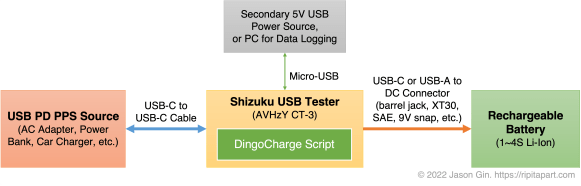
The Shizuku USB multimeter by YK-Lab, which is available in a few rebadged forms under names like YK-Lab YK001, AVHzY CT-3, Power-Z KT002, or ATORCH UT18, is a very useful USB charger testing device. It features USB-A and USB-C ports; can measure voltage, current, power; can calculate passed charge (mAh) and energy (mWh) in real time; but unlike most USB testers on the market, it is user-programmable in Lua, a lightweight programming/scripting language.

The Lua API on the tester provides a large amount of extensibility beyond the original tester’s design, and in my case I’m using its ability to “trigger” non-standard voltages from fast-charge capable power adapters as well as its colour LCD screen to act as a highly flexible direct charger – an intermediate between a USB-C PD PPS adapter and an arbitrary (Li-ion) rechargeable battery.

Introducing: DingoCharge!

The idea behind making a battery charging script came about when I looked at using bench-top adjustable power supplies to charge batteries. Since the Shizuku tester (in my case, it was the AVHzy CT-3 variant) allows me to use the PPS protocol to finely adjust the adapter’s output voltage, I tried manually varying the voltage to increase or decrease the current flowing into a battery – and it worked!

That said, constantly checking the battery’s current and voltage levels just to charge a battery gets pretty tiring, and since the Shizuku is Lua-programmable… why not make a script that automates all of this for me? Thus began a programming journey that’s been ongoing for over a year, and I’ve still got ideas to add even more functionality (as long as I don’t crash the tester by running out of memory… don’t ask me how I know).

Charge Regulation Algorithm

All lithium-ion batteries (including less-common ones like lithium-iron phosphate (LiFePO4) and lithium titanate) use what’s known as CC-CV charging; this stands for constant-voltage/constant-current. A fixed amount of current is fed into the battery until its voltage reaches a certain threshold, then the voltage is held at a fixed value until the current going into the battery drops below another, lower, threshold. Once this is reached, the current is turned off entirely and the charge process is complete.

Although the PPS specification allows a device to set a maximum current level, my own testing revealed that there was too much variation amongst all my different adapters that I could not rely on the hardware to perform the constant-current regulation with enough precision for my liking, and the voltage drop across the USB-C cable resulted in the battery’s charge current tapering off too early as the voltage at the adapter reached its programmed constant-voltage level before the battery’s own voltage had a chance to do so as well. Instead, my charge algorithm increases the requested USB PD charge voltage above the battery’s own voltage until the desired current level is within a certain deadband range.

Once the target constant-voltage level is reached, the charge algorithm switches to constant-voltage regulation, maintaining a preset voltage until the current being drawn by the battery falls below the termination threshold.

If a battery was previously overdischarged, it requires a slower “precharge” current to bring the battery’s voltage up to a level that is safe for its regular charge current.

Charge Safety Tests

Over time, I added more safety checks to ensure that the battery’s state was maintained within a safe margin for voltage, current, temperature, and also time. If a safety violation was detected during charging, the charging algorithm would automatically set its charge current to zero, effectively terminating the charge process. Additionally, if the charge process was finished but a small current flowing into the battery resulted in the battery’s voltage getting too high, the PD request voltage gets adjusted downwards to prevent an overvoltage condition from occurring.

Downstream Resistance Compensation

I also added the ability to compensate for high-resistance connections to the battery. This works by using Ohm’s Law (voltage = current * resistance) to boost the voltage thresholds in proportion to the amount of current flowing into the battery, as determined by a configured downstream (tester-to-battery) resistance. This is usually considered an advanced feature for a charging system, but since all of the charging is handled in software, it is relatively trivial to allow for compensating for lossy cabling and connectors.
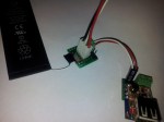
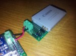
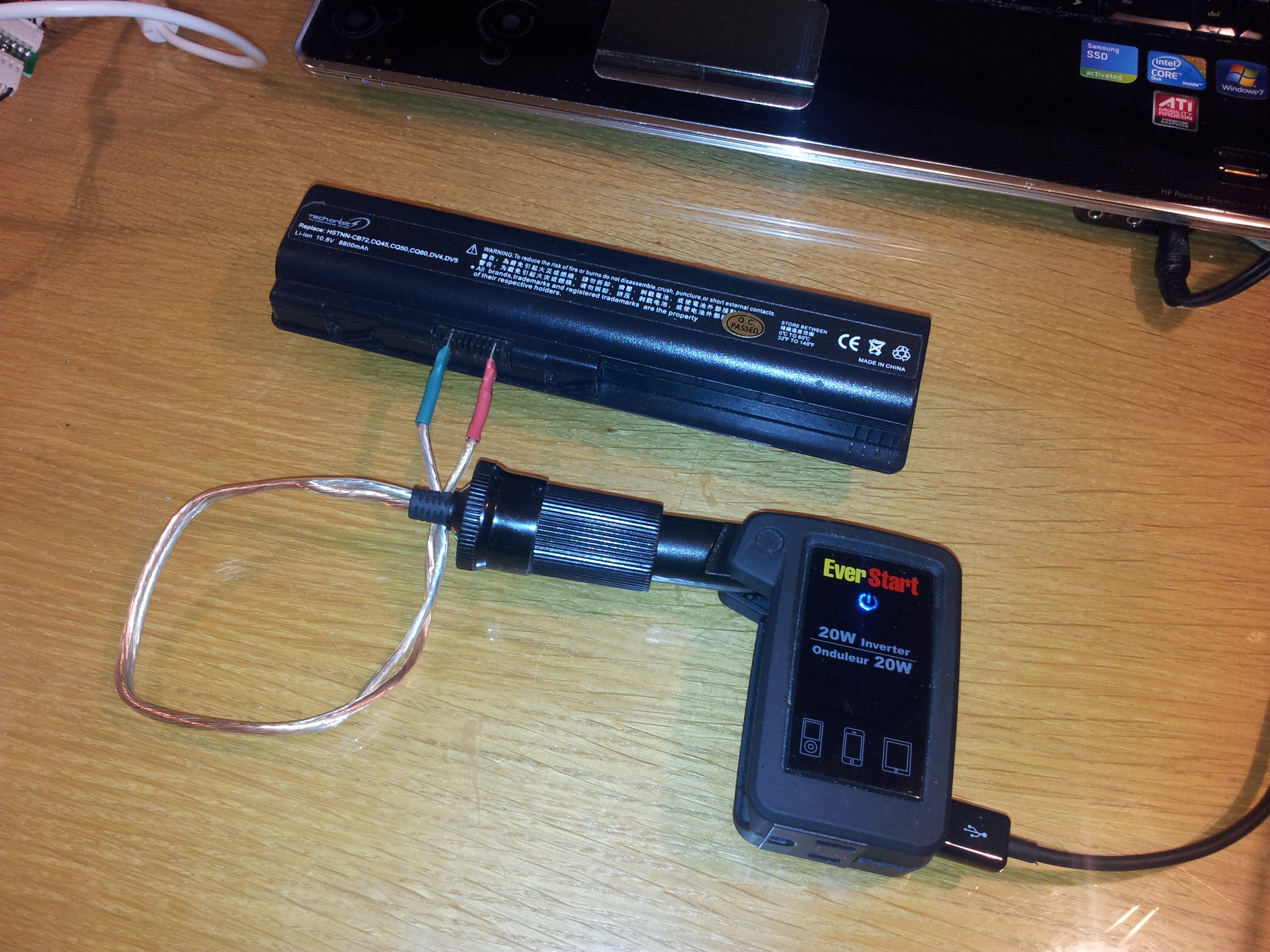
Charging Test

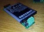
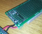
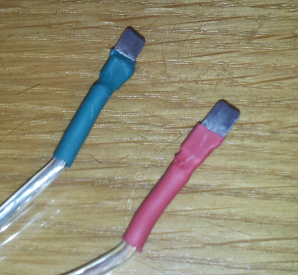
As a real-world demonstration of the DingoCharge software, I created a test setup that charged a 600mAh/7.4V nominal battery pack (a rechargeable 9V alternative that’s built from disposable vape batteries – stay tuned for that blog post!) at a 1C (600mA) rate at 8.4V (4.2V per cell) until the current tapered off to C/10 (30mA); note that the pack I was charging was built with high-drain cells that can handle higher currents than normal, and most commercial cells are best charged at a C/5 to C/2 rate. I used a Samsung EP-TA800 USB-C adapter, capable of a maximum of 25W at full power (11V at 2.25A).

Demonstration of DingoCharge charging a 9V Li-ion replacement, using a Samsung 25W USB-C PD adapter.

Demonstration of DingoCharge charging a 9V Li-ion replacement, using a Samsung 25W USB-C PD adapter. (click here for full-size image)

Block diagram describing the DingoCharge hardware setup.

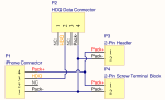
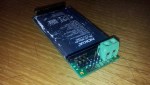
Block diagram describing the DingoCharge hardware setup. All power conversion (and associated power conversion losses) occur only in the power source, with the tester simply issuing commands to control the power going into the battery. (click here for full-size image)

Voltage/current plot of DingoCharge charging a battery at 600mA and 8.4 volts, using a Samsung EP-TA800 USB-C PD adapter.

Voltage/current plot of DingoCharge charging a battery at 600mA and 8.4 volts, using a Samsung EP-TA800 USB-C PD adapter. (click here for full-size image)

The classic CC-CV charge profile is visible when the charging current and voltage is graphed over time. The stepped nature of the current is a consequence of the PPS voltage being limited to 20mV granularity, causing jumps in current draw as each step occurs. The voltage is increased or decreased when the current or voltage being sent to the battery falls out of a certain range (in this case, 600mA and a +/-25mA deadband during constant-current charging, and 8.4V +/- 10mV during constant-voltage charging).

One contribution to the relative flatness of the constant-voltage phase is that the charging algorithm is essentially performing four-wire (also known as Kelvin) sensing from the adapter to the tester, inherently compensating for voltage drop across the USB-C cable. This is also why the current flutters a bit as it tapers off, as the voltage at the battery begins to rise above the deadband, resulting in a small amount of oscillation as the algorithm tries to maintain 4.2 +/- 0.01 volts.

Limitations

Nothing in this world is perfect, and neither is my charger implementation. In fact, trying to shoehorn a battery charger into what’s effectively a multimeter and a “wall wart” required a lot of compromises to be made.

No Power Switching

Charge termination is a bit tricky, as most implementations will just electrically disconnect the battery. However, with the tester, there is no power switching available that can be controlled through software. This is mitigated by setting the constant-current algorithm to 0 amps +/- 10 milliamps, resulting in minimal charge/discharge current as the battery voltage drops while it relaxes from a fully-charged state.

One Name, Many Variations

Another limitation is that the PPS protocol allows adapters to not necessarily support the full voltage range of 3.3 to 21 volts. Instead, there are options to support up to 5.9, 11, 16, and/or 21 volts, and at current level up to 5 amps. The large disparity of supported voltages and currents means that the DingoCharge script needs to check the programmed charge parameters against what the adapter supports; many PPS adapters only support up to 11 volts, so 3S (3 cells in series) and higher cell configurations will not work (and an error message will be displayed if that is the case).

My (Electro)chemical Romance Recharge

I designed DingoCharge only for use with lithium-ion type battery chemistries, but have been experimenting with charging other rechargeable batteries, such as lead-acid and nickel-metal hydride/Ni-MH. There has been promising results with both chemistries, but each one is not fully supported as I have not implemented proper 3-stage charging for lead-acid batteries; Ni-MH charging only works by using a low current (C/10 typical) for a fixed period of time via DingoCharge’s time limit feature, or an external temperature sensor alongside the overtemperature protection feature to stop the charge process (a very crude delta-T/change-in-temperature algorithm). Thankfully, the software-based approach of DingoCharge means I can add this functionality in an official capacity with further research and development work… as long as I get around to it 😛 .

Lua Lunacy?

Additionally, this was my first real foray into Lua programming, so I’m pretty certain I’ve made some poor stylistic and other programming choices along the way. For all I know, it could have inherited some significant syntactic defects from my other programming (language) attempts that make it an “awful” program – but hey, it’s an open-source project so if you have some pointers, feel free to help contribute on GitHub (link is in the Downloads section below)!

Conclusion

The USB PD protocol, and its adjustable PPS functionality that was introduced in the PD 3.0 specification, provides a lot of potential use for directly charging batteries since it skips the usual conversion step in a device. However, this type of charging technology was largely untapped by many devices, with only a few smartphones (as of the time of writing) supporting it.

The scriptability of some USB-C testers like the AVHzY CT-3 or Power-Z KT002 allows for a script to handle all of the intricacies of battery charging, while providing an easy-to-use yet highly flexible interface. Thanks to the DingoCharge script, any USB PD PPS adapter and supported USB tester can be used as a universal battery charger.

Downloads

The DingoCharge script can be found on my GitHub profile (https://github.com/ginbot86/DingoCharge-Shizuku), and is open-source under the MIT License. If you have a suitable USB PD PPS adapter and USB-C tester, I’d love to hear if/how well DingoCharge works for your batteries!

Atomic Pi Adventures, Episode 1: Adding external PCI Express expansion by removing onboard Ethernet

As seen on Hackaday!

TL;DR: The Atomic Pi single-board computer CAN be expanded through PCIe. It’s just a massive pain to do so, even if you have steady hands. Let’s just say it’s a long story…

DISCLAIMER: The modification performed in this blog post can, and has, caused permanent hardware damage to my Atomic Pi, albeit repairable with much skill and effort. Reenacting what I’ve done requires significant experience with SMT (surface-mount technology) components, some barely larger than a grain of sand (I consider 0402-size components to be “oversize” in this instance). I accept no responsibility for damages arising from attempting this modification.

Introduction

Single-board computers (SBCs) are all the rage nowadays, with the Raspberry Pi being the most well-known in this category. SBCs are compact computers, carrying their own CPU and memory, and usually some on-board storage and various I/O connections (e.g. USB, HDMI, Ethernet). Most of these computers use the ARM architecture, found on almost all mobile devices today. However, some use the x86 architecture, which is used in higher-end tablets, laptops and desktop computers.

Recently, the Atomic Pi made waves in the electronics hobbyist space, boasting an Intel Atom Z8350 quad-core CPU with 2 GB of RAM, 16GB of eMMC storage, Gigabit Ethernet, Wi-Fi, USB 3.0, built-in speaker amplifiers, and lots of general-purpose I/O (GPIO) pins – all for less than $40 USD!

As one might expect, there were caveats to this little computer, with some dismissing it very harshly, if not unfairly. With some investigative work, members of the community found out that the “Atomic Pi” board actually belonged to the Kuri robot from Mayfield Robotics; the company shut down in late 2018, and the liquidated stock of these SBCs were snatched up by Digital Loggers with the help of a Kickstarter campaign, who then developed breakout boards to make using them easier. This is because – unlike almost every other SBC – you can’t just plug in a barrel jack or USB cord to power it! Instead, it uses a 2×13 pin header, which many users did not have on hand, nor had the skill and/or resources to build their own solution. This is compounded by the board’s need for clean, well-regulated 5 volts at 2-4 amps, with 12 volts being optional to power the onboard speaker amplifier. The 16 gigabytes of eMMC storage proved to be too cramped to run Windows 10 directly, and the Realtek RTL8111G Gigabit Ethernet chipset is often frowned upon by those in the pfSense (a free firewall/router OS) community.

The NIC’s usage of the Z8350’s single PCI Express (PCIe) lane is what caught my attention. Unfortunately, the RTL8111G Ethernet chip is soldered to the board, with no easy method to replace it with an external card. A few people have attempted to remove the chip and wire in an external PCIe riser, without success. With my previous experience with fine-pitch electronics work, I figured that this would be a fairly easy modification to make.

It wasn’t. In fact, this was one of the most frustrating electronics projects I’ve done to date – and now you get to come with me in my adventures (and misadventures) in microsoldering on the Atomic Pi (or was it Kuri? The jury seems to be out on the nomenclature).

Optional Reading: PCI Express Signals

PCI Express (or PCIe for short) is a very common high-speed interface for connecting processors or chipsets to all sorts of different peripherals. It uses low-voltage differential signaling to minimize interference, and a single lane of PCIe can carry 250 MB/s for the first generation, all the way up to 2 GB/s for the fourth generation!

A single PCIe lane is made up of three differential pairs: receive, transmit, and a 100 MHz reference clock. Control signals for waking up and resetting peripherals are also provided. Riser cards, often used for cryptocurrency mining, use these five signals to provide the minimum connectivity for any PCIe peripheral. The interface is highly flexible, allowing graphics cards that normally use 16 lanes to run on just one lane. The specifications for PCIe make board design easier, as the differential lines are designed to adapt to different lane configurations; the polarities in a pair (transmit, receive, clock) are polarity independent (all that matters is that you maintain a good differential pair).

PCIe Signal Pinout

Since the Atomic Pi lacks a PCIe slot of any kind, I have provided the diagram indicating which signals go to what points on the board:

Note that the AC coupling capacitors are required for the peripheral Rx (receive) pair, and are optional for the peripheral Tx (transmit) pair.

Attempt 1: “Chipple” Bypass

I started this project with the intent of making my modifications as reversible as possible. Looking at the RTL8111E’s datasheet (a similar model to the 8111G) revealed the presence of an “ISOLATEB” pin; grounding this pin causes the chip to disable itself and release its hold on the PCI Express lines.

This brings us to the first roadblock: the Ethernet chip is soldered to the board, and the components that connect it are known as 0201 (0.002 inches in length, 0.001 inches in width), smaller than a breadcrumb!

After disabling the Ethernet chip, I used my trusty 0.1mm (that’s four-thousandths of an inch!) magnet wire to tap into the PCIe lines, and brought them out to a PCIe riser card, which provided a USB 3.0-type socket for an external connection.

Unfortunately, high-speed signals aren’t just about wiring from one device to the next, and this was no exception. The rat’s nest of wires were no suitable medium for the 5-gigabit signals to traverse (PCIe requires very tight control of electrical trace layouts), and the Atomic Pi was unable to detect the presence of any device on the external PCIe port.

Attempt 2: Thin Twinax Troubles

With the signaling issue in mind, I tried some very thin twinaxial cables from a dead MacBook’s hard drive cable to connect the PCIe lines to my riser card. This cable is very thin, with an outer thickness similar to fishing line. It uses a foil and wire “shield” around the two internal wires to protect it from external interference. I figured that this should help protect the delicate signals from the harsh outside world.

I didn’t have very much of this thin twinax cable on hand (that said, if anyone knows where I can buy this stuff in bulk, please let me know!), so I was limited to very short lengths for each pair. I ran out of twinax after the transmit and receive pairs, and resorted to using two coaxial cables from that same cable bundle.

After fiddling with the super-thin wires and soldering them to the header, I still got nowhere and could not get the Atomic Pi to see an external PCIe card.

Removing my modifications revealed my first blunder: despite placing the chip into a temporarily disabled state, the Ethernet chip was dead! This meant that I could not use the built-in Ethernet port anymore, and the LEDs next to the Ethernet port simply glowed a dull orange instead of their rapid blinking pattern when data is being transmitted over Ethernet. I figured that there was no use keeping the chip on the board, so I used my hot air rework station to remove it, using a generous amount of heat and flux to get the chip removed.

Attempt 3: To Ribbons, You Say?

With the dead Ethernet chip removed, I decided to use another tactic to bring out the PCIe interface. I decided to use a thin ribbon cable (okay, more accurately a “flat flexible cable”) to help decouple any mechanical stresses from moving the external USB 3.0 connector around during testing, and its compact size allowed me to try using the QFN pads to connect my ribbon cable, hopefully minimizing noise that could be picked up, as well as avoiding any “stubs” of wiring within the differential pair that would degrade the signals.

The challenge is that the chip uses a very small pad spacing, and I wanted to avoid soldering directly to the ribbon cable. I managed to salvage a couple connectors from some other devices, and used a cut-up CompactFlash memory card’s PCB to make it easier to solder the connector, as well as provide a base for the connector to sit on.

The connector on the board was affixed onto the Ethernet chip’s footprint with the help of some double-sided foam tape, and magnet wire was used to bond the PCIe signal wires onto the ribbon cable. The ribbon itself used copper foil on one side to help with interference suppression, and provide the signals a “ground plane” to travel across.

Things weren’t quite as elegant on the other end of the cable, however. I still had to contend with a fine-pitch ribbon connector, and a way to connect that to a male USB 3.0 plug to hook it up to the PCIe riser. I had little option except to use the small lengths of twinax from the last attempt, and (perhaps unsurprisingly) it didn’t work.

Attempt 4: Teeny Tiny Twists

The next attempt went to a smaller scale, using a very fine twisted pair I created out of my 40 AWG magnet wire (each wire is as thick as a hair). I then shielded this magnet wire by sandwiching it between pieces of copper tape to act as a ground plane for the signals. I reused a dead USB 3.0 drive to act as the plug for the PCIe riser, and wired it straight to the QFN pads of the original Ethernet chip.

Although the twisted pair would have, in theory, reduced intra-pair skew and some degree of EMI resistance thanks to the copper tape, the homemade twisted pair almost certainly would not have provided a 100-ohm differential impedance that’s required for PCIe signaling. Once again, the attempt to break out PCIe from the Atomic Pi was a failure.

Attempt 5: SASsiness Yields Results…?

Since the central issue with external PCIe connectivity involved the connection between the Atomic Pi board and the riser, I figured I would try a medium that was specifically intended for high-speed differential signals. I bought some thin SATA cables (specifically the 18-inch thin cables on Amazon), which used two pairs of thin SAS cable per SATA connection. The difference between SATA, SAS and PCIe is of little difference here, as the key criteria was a differential pair with 100-ohm impedance and ability to carry high-frequency signals.

Despite being a thin cable (each conductor is only 30 AWG, or 0.25 mm in diameter), these cables were too stiff to directly connect to the AC coupling capacitors without a very high risk of damaging the capacitor and/or the pad it is soldered to. I had to reinforce the cables by soldering them down and hot gluing the cables to the board at multiple points to relieve stress on the connections.

The original 0201-sized AC coupling capacitors were removed, and more reasonably-sized 0402 capacitors were used in their place. Each capacitor was a common 100nF capacitance, and were easy to harvest from some dead laptop motherboards I had on hand. I “flipped” the layout of the capacitors away from the QFN footprint, but this meant that only one side of the capacitor was actually anchored to the board; this made the capacitors very fragile and I often lost the terminations on the capacitors (thankfully they are plentiful in electronic devices like this).

To help minimize stress on the vulnerable capacitors, I used magnet wire as a flexible “bridge” between the capacitor and the SAS cable, and the cables were tied down to solder tab wire that I used as “bus bars” for a strong electrical ground as well as a tie-down point to take away most of the strain of the cable’s flexion. Despite negatively affecting signal integrity, I was able to get a sufficiently stable connection to perform some initial testing, and I succeeded! I was able to connect an Intel 82576-based dual-port network card to my external riser.

However, this didn’t last long. The simple movement of the wires on the board when trying to connect different peripherals was enough to break the AC coupling capacitors, despite the use of my flexible terminations from the SAS cable to the capacitors. Replacing the damaged capacitors and redoing the magnet wire terminations failed to restore connectivity, so I desoldered all of the existing connections and started over.

Attempt 6: We Have Lift-Off! (that’s bad)

In an attempt to further improve signal integrity, I decided to take the bold move of eschewing the flexible terminations of magnet wire, and decided to directly solder the SAS cable’s wires to the capacitors, which are soldered to the PCIe pads on the Atomic Pi. I anticipated that physical stresses would damage the capacitors, so I opted to use longer lengths of SAS cable, and to hot-glue the cable to the board at regular intervals to minimize the amount of stress that gets coupled into the cable and capacitors. The 100 MHz reference clock continued to use magnet wire for connection as it was at a much lower frequency than the PCIe signals, and reduced the amount of physical crowding around the PCIe pads.

This leads me to my next issue. To help with structural integrity, I repositioned one of the SAS cables so that it would remain on the board before going to the PCIe riser connector, meaning it would be perpendicular to the other cables. This required me to strip extra foil shielding to jump over the existing capacitors, which increases the risk of physical stress on the capacitors, as well as reduced signal integrity. Additionally, I used a longer set of twinax cables, sacrificing two SATA cables to get most of the original 18 inches of length per cable.

Testing of this construction method failed, and it was only at this point that I realized that two of the four AC coupling capacitors I used weren’t the same capacitance; PCIe usually uses 100 nF capacitors, but I had a 1 nF on one PCIe pair, and 10 nF on the other – no wonder things weren’t communicating (and that’s what I get for assuming the capacitors were the same)! Unfortunately, the process of removing the SAS cable connections resulted in the phenomenon I was trying to avoid: the board’s PERp0 (the positive side of the PCIe receiver) pad had lifted away from the PCB, leaving me with an unsolderable crater.

Attempt 7: Success!

After losing one of the pads for the original coupling capacitors, I was feeling pretty defeated. I didn’t let this stop me, and I decided to apply my magic skills with 40-gauge magnet wire to the trace, and was able to get a sufficient connection with a replacement 100 nF capacitor (and this time I measured it…), hopefully in such a way as to not too negatively affect signal integrity. Unfortunately, the 0201-sized resistors used to connect the PCIe reset and wake signals lost their terminations and no longer took solder on one end; I opted to keep the resistors in place and soldered magnet wire to the other end (facing the SoC rather than the Ethernet chip), as further measurement revealed that the resistors were simply 0-ohm jumpers anyway. I scrapped the longer SAS cables, and went back to the ~8-inch lengths to reduce attenuation.

After rewiring the PCIe data, clock and control lines, I crossed my fingers and retried the riser with my Intel NIC – and it worked! After verifying the connections were sufficiently strong, I decided to make the modification permanent, and covered the area with epoxy to prevent any of the components from breaking loose. Additionally, I used some aluminum sheet metal, double-sided foam tape and some zip ties to create a reinforcement bar, helping to strengthen the cable connections as they leave the board.

With all the connections in place, it was time to get to the fun part: seeing what PCIe peripherals work on the Atomic Pi!

Testing Results

One interesting behaviour of the Atomic Pi when using Windows is that changing PCIe cards often causes the system to immediately power down or freeze during boot. Simply powering the board on again seems to fix this issue. Why am I using Windows? I already upgraded the board to a 64GB eMMC instead of the original 16GB, and the appeal of the Atomic Pi’s x86 architecture was the ability to run desktop apps – in particular, Windows apps.

The UEFI firmware has a hidden advanced menu, accessible if the “shutdown /r /fw” command is run as administrator. There is a section for PCIe settings, and the ones that interested me were the AER (Advanced Error Reporting) and PCIe hot-plug settings. Unfortunately, these do not seem to have any effect as Windows doesn’t seem to pick up any hardware events in the Event Log.

Test 1: Network Devices

PASS: Intel 82576 Dual-Port Adapter

If the port(s) have a connection to another device (e.g. a network switch), the orange and green LEDs will illuminate soon after the PCIe link is properly initialized, which makes for quicker troubleshooting. Even if the system is off, the green link LED remains lit, but goes out once the PCIe bus is reset.

The card works a treat in pfSense and Windows, allowing high-performance Gigabit-speed transfers with both ports in use. However, the UEFI firmware does not recognize the card as a bootable medium (which is for the best in my opinion – the PXE boot program tends to hinder the boot process more than anything).

PASS: Realtek RTL8111GS (External Card)

The PXE network boot program built into the UEFI firmware works just fine, which is expected as the chip is the same type as the original RTL8111G, with the exception that the chip has a built-in switching converter rather than the linear LDO that the Atomic Pi uses natively.

PASS: JMicron JMC250

The card works in Windows and pfSense; the particular card I have has always been flaky in operation, and this was no exception.

PASS: ASUS PCE-N15 (Realtek RTL8192CE) 802.11n WLAN Adapter

Using this card is a performance downgrade compared to the dual-band adapter already present on the Atomic Pi, but it did function correctly in Windows.

Test 2: External Graphics Cards (eGPU)

PASS: EVGA/nVidia 8500 GT

The UEFI firmware doesn’t seem to want to acknowledge the presence of PCIe graphics adapters, which results in issues when testing in Windows. Initially, the card failed to enumerate correctly, identifying as a Microsoft Basic Display Adapter and displaying an error in Device Manager:

This device is not working properly because Windows cannot load the drivers required for this device. (Code 31)

The driver trying to start is not the same as the driver for the POSTed display adapter.

Manually downloading and installing the drivers allowed the card to work properly. As previously mentioned, the UEFI does not recognize the presence of the graphics card, so a monitor that is plugged into the graphics card won’t start working until Windows is loaded and the graphics driver initializes.

Additionally, the adapter’s resources won’t be used if the monitor is connected to the Atomic Pi’s built-in HDMI port – it’s a tradeoff between graphics performance and the ability to see what’s happening on boot; maybe this is different in a multi-monitor configuration, but I didn’t have enough desk space to test this.

PASS: XFX/AMD Radeon 4650

The same driver issues popped up when using this card as well, and the same fix applies.

PASS: ASUS/nVidia GTX 660 Ti

Ditto. This card was the best I had on hand for testing, and amusingly it consumes about 10-20 times the amount of power that the Atomic Pi uses, and is bigger in size as well.

Connecting this card allowed me to run games that would otherwise simply not work, such as Just Cause 2. It performed at about 20-30 frames per second: not great but not terrible. Just Cause 3 was absolutely painful to run, but this is not surprising as the Atomic Pi’s hardware is far below the game’s minimum requirements in almost all aspects.

Test 3: Storage

PASS: Dell PERC H200 SAS Adapter

To my surprise, not only will it work in Windows, it even supports booting from the UEFI! It mentions a SAS controller driver during boot, but I am not sure as to whether this is present in the Atomic Pi’s UEFI, or if it is a driver provided by the SAS adapter itself. The PCIe 2.0 1x interface limits the maximum throughput to less than 500 MB/s, which is slower than a single SATA III connection, and informal testing showed a maximum speed of about 330 MB/s. I have not investigated whether I could configure the hardware RAID features of the adapter from the operating system, but I imagine that doing so would dramatically improve performance when running a RAID 1 (mirrored) setup.

FAIL: OWC (What’s This?) Aura Pro X 480GB NVMe SSD

This SSD was originally meant as an aftermarket SSD upgrade for a MacBook Air, but I bought a PCIe adapter card to use it in a regular PC. I was able to get it to enumerate in Windows, but any sort of read/write action caused it to lock up and throw errors in the Windows Event Log. I suspect this is likely a power supply issue due to how the PCIe riser board provides power (12 volts -> DC/DC converter -> 3.3V LDO linear regulator), or maybe the card just doesn’t want to cooperate.

FAIL: Marvell 88SE9128 2x SATA III + 1x PATA UDMA-133

This adapter caused Windows to almost freeze during boot. Instead, the boot animation would advance by one frame every 2 seconds until the card is removed. I suspect this is the PCIe bus attempting to negotiate a connection but failing, possibly due to signal integrity issues. Checking the Windows Event Log turned up nothing either.

Test 4: … More PCIe?

FAIL: Extender Cable

One would think that a simple straight-through cable would work, right? Nope – it seems like the signal has already been degraded enough after traveling across multiple non-ideal connections, and the extra length in a cable was just enough to degrade the signal beyond recovery.

PASS: PCIe Port Multiplier / ASMedia ASM1184e

UPDATE (July 3, 2019): It seems that the “USB 3.0” pinout on these PCIe risers is inconsistent. I was somehow able to make do by using a PCIe card plugged into my current riser, which then led to the ASM1184e board, which splits the PCIe 2.0 1x lane into four slots. It seems like the chip is able to handle the attenuation over such a long cable length, and it even includes a 100 MHz clock buffer, effectively “refreshing” the signal for more sensitive PCIe cards.

I tried the 88SE9128 card again, but still had no luck. Ethernet cards worked without issue, but I wasn’t able to test the graphics cards as the ASM1184e board’s PCIe slots are closed-ended 1x slots. I could try cutting the edge of the connector to allow for larger cards, but that’s an experiment for another day.

Conclusion

Despite all the roadblocks I encountered in this project (sometimes rage-inducing ones), I still enjoyed this project and the various techniques I tried along the way. The prospect of attaching desktop PCI Express peripherals to a CPU designed for a tablet opens up many different applications for the Atomic Pi, including ones that would otherwise have been less efficient or impossible using the board’s built-in hardware (e.g. dual Gigabit Ethernet without using USB, or GPU-intensive computing workloads).

The high-speed nature of modern computer systems presents many challenges for engineers and modders alike. Multi-gigabit interfaces easily reach into the realm of radio-frequency (RF) electronics, where things like AC transmission line effects and differential signal routing become very important. This issue, coupled with the fact that most modern devices use very small components, makes it difficult for many electronics hobbyists to access these interfaces on their own. Although a modification like what I did is technically possible, I don’t consider it practical for an average electronics/computer enthusiast.

Future Ideas

One avenue I’ve thought about pursuing is a mod board that is soldered onto the Atomic Pi’s PCB, allowing a more robust connection for the PCIe lines; this would include signal integrity improvements like ESD protection and PCIe line redrivers to strengthen the signals to/from the SoC and peripheral(s). PCB design is currently beyond my scope of knowledge, but it would be a fun way to dive right into the subject matter.

Performing safer AC line voltage measurements using isolated amplifiers

DISCLAIMER: AC line (mains) voltage is not something to be taken lightly! Attempting to safely handle line voltages while minimizing the risk of harmful or fatal electric shock is the main motivator for me to design and build this circuit. However, I am no electronics engineer and I definitely have no formal training on international standards pertaining to high-voltage safety. I accept no responsibility, direct or indirect, for any damages that may occur if you attempt to make this circuit yourself, including personal harm or property damage. Additionally, there is no warranty or guarantee, express or implied, on any content pertaining to this blog post (or any other posts).

UPDATE (November 19, 2018): Added isolation voltage ratings for the amplifier and DC-DC converter.

As seen on Hackaday!

Back in mid-2017 I won a Keysight DSOX1102G digital storage oscilloscope (DSO), a piece of equipment long on my wish list but never acquired until then. One thing I’ve wanted to be able to measure with an oscilloscope for a long time was the waveform of the AC utility (in other words, the wall outlet). However, doing so presents a very real risk of blowing equipment up or shocking yourself (and possibly other people). In order to prevent this, I needed a way to perform measurements on the AC line without being directly connected to it; in other words, I need galvanic isolation.

Isolation Methods

There are many different ways to achieve galvanic isolation. Common methods are the use of transformers and optocouplers, but they each have their own disadvantages.

Optocouplers (aka optoisolators) are a common component used for isolation, but they require a fair bit of external circuitry to work correctly – not to mention its current transfer ratio (CTR) varies with temperature and age, resulting in drifting measurements over time if a feedback circuit isn’t used. They also aren’t very fast; the common Sharp PC123 optocoupler has a cutoff frequency of only 80 kHz and a response time of 3-18 µs (but newer ones can be much faster).

Transformers don’t require active circuitry and would make stepping down voltages simple. However, their inductive nature causes issues when measuring waveforms with low-frequency content and sharp edges (like the output from modified sine wave inverters), resulting in inaccurate measurements due to the ringing and other distortion that the transformer creates. Additionally, common iron-core transformers aren’t very good at capturing frequencies above 20 kHz.

Solution: Isolation Amplifiers!

I settled on using an isolation amplifier to provide the necessary protection from the AC line and the oscilloscope. Several years ago TI provided sample kits for electronic motor drives, with one component being the AMC1200 isolation amplifier; this is the IC that I used in my AC waveform viewer – however, note that there are some limitations that I will address later in this blog post.

The AMC1200 uses TI’s digital capacitive isolator technology, using high-voltage SiO2 (silicon dioxide) dielectric capacitors on the chip itself for high voltage protection. The amplifier’s input is essentially digitized using a sigma-delta modulator, whose output is then sent digitally across the isolation barrier before being demodulated back into an analog output. It is rated for a working isolation voltage of 1200 Vpeak (848 Vrms), and a maximum isolation voltage of 4000 Vpeak (2828 Vrms), well above the typical voltages experienced on a 120V line.

AC Waveform Viewer Construction


As with most of my projects, my AC waveform viewer is built on FR4 fiberglass perfboard. The isolation components used are the AMC1200 isolation amplifier by Texas Instruments, and its corresponding power supply is the NXE1S0505MC isolated DC-DC module by Murata. It is rated for reinforced insulation up to 125 Vrms and basic insulation up to 250 Vrms, with a production-tested Hi-Pot rating of 3 kVDC. It does provide reinforced insulation at the voltages used in North America, but is still the weaker link in terms of maximum isolation voltage.

The AMC1200 features differential inputs and outputs, with a maximum input voltage of +/- 200 mV intended for use with low-resistance current shunt resistors.

One potential problem with perfboard is that the through-holes compromise the high-voltage isolation of the circuit (reducing the creepage and clearance distances), acting as multiple series spark gaps. The solution to this is similar to how isolation slots are used on commercial PCBs; that is, drill out the holes! This greatly increases the distance between each side of the circuit and improves the safety of the circuit.

The AC voltage input is scaled down to a manageable level via a resistive voltage divider. I used four high-precision 300kOhm resistors in series, plus a 1kOhm resistor placed across the AMC1200’s input terminals. Since the input is floating thanks to galvanic isolation, I decided to place the amplifier’s input in the middle of the voltage divider (that is, 600kOhm of resistance is present from the neutral and line terminals) to provide some extra protection from harmful electric shock; 120 Vrms / 600 kOhm = 0.2 mA to ground is the maximum amount of current that could possibly flow if I were to contact this floating node on the amplifier (this calculation assumes that my body has zero resistance, but human skin resistance is generally much higher than this). The voltage divider and the AC input terminals of my waveform viewer are further insulated with a layer of clear epoxy for even more protection.

The power supply terminals are fused with a 500 mA fuse before being protected by an SMAJ5.0A TVS (transient voltage suppression) diode and filtered with a 22 uF tantalum capacitor. The AMC1200’s output terminals are protected with 5.1 V Zener diodes at the terminal blocks for ESD and overvoltage protection.

Due to the floating nature of the waveform viewer, this essentially is a differential probe for my oscilloscope (and most high-voltage differential probes actually aren’t isolated!).

Circuit Limitations

No circuit is perfect, and mine is no exception. Here’s a few issues with my circuit that I’d like to address:

Isolation limitations

The AMC1200 only provides “basic insulation“; that is, it will provide protection from electric shock as long as its insulation barrier is not damaged (in other words, there is no redundancy). Circuits that have terminals that can be directly touched by humans needs “reinforced” or “double” insulation to be compliant with international regulations.

The NXE11S0505MC isolated DC-DC converter has a maximum working voltage of 125 Vrms for reinforced insulation and 250 Vrms for basic insulation, with a Hi-Pot test at 3 kVDC. This is lower than the AMC1200’s maximum voltage of 4000 volts, but these should still have enough headroom to keep me safe in the event of a mild voltage spike. It might prove useful to add some sort of surge suppression with a MOV (metal oxide varistor) or similar device.

The perfboard layout is also sub-optimal for the sake of isolation. Despite drilling out a row of holes to increase the creepage and clearance distances, it isn’t quite enough to meet regulations, as the clearance is only 3 mm and the the creepage isn’t much better, around 4 mm. This is still more than enough to withstand normal AC line voltages, but there is always a chance that higher-voltage transients will make their way onto the line and the isolation barrier needs to take this into account.

Output limitations

The AMC1200 provides a differential output that is centred (common-mode voltage) at 2.5 V, which can be an issue with single-ended inputs like that on an oscilloscope. I’ve worked around this by using a floating power supply, like a USB power bank, and connecting the oscilloscope’s ground terminal to the AMC1200’s Vout- pin. Also, the AMC1200 has a limited bandwidth of 60-100 kHz, but for the purposes of waveform monitoring it is sufficient; however, the amplifier’s noise and offset also negatively impacts performance as the high attenuation ratio essentially amplifies these values to the point where the AC waveform looks like a 2 Vdc offset and the noise level is so high that I need to use the averaging or high-resolution acquisition modes on an oscilloscope to get a clean waveform.

Power supply limitations

The NXE1 isn’t quite suited for such a low-power task as operating a single amplifier input. According to the datasheet, the output voltage can rise to twice the rated voltage if it is loaded with less than 20 mA. To combat this, I placed a 5.1 volt Zener diode across the output to provide regulation, which unnecessarily wastes power. Another regulated module like the NXF1 series would be a better choice, and the unit cost at one-off quantities isn’t a huge deal either.

Room for improvement

With this circuit working properly, I had plenty of ideas to make the second iteration even better:

Simultaneous voltage/current inputs

With the ability to measure current, I can perform measurements on the current draw of a device, allowing me to determine the power factor of a device.

True single-ended outputs

Most ground-referenced devices like oscilloscopes are not meant to handle differential inputs directly. Multimeters, especially battery-powered ones, are an exception.

Reinforced insulation rating on amplifier

The AMC1200 is only rated for basic insulation, so having an amplifier rated for reinforced insulation would provide greater electric shock protection. Alternatives like the Silicon Labs Si8920 could be a viable solution.

Waveform captures


Conclusion

Despite its ubiquity, AC power is a force that must not be taken lightly. Performing measurements on it, especially when viewing its waveform on a non-isolated oscilloscope, requires extreme caution as line voltage (especially in countries where 230 V is common) can easily injure or kill.

Using a voltage divider and isolation amplifier allows for safer measurements of the AC line without introducing distortion, especially compared to transformer-based implementations; this is critical when measuring the waveforms of modified sine wave inverters.

My implementation of an isolated differential probe helps protect me from electric shock when making measurements, while costing much less than a commercial high-voltage differential probe (for example, the CT2593-1, costs almost $330 USD on DigiKey).

But… which one would you trust more?

eMMC Adventures, Episode 3: Building a custom adapter to use cheap eMMC-based 32GB SSD modules

As seen on Hackaday!

While on my quest for more eMMC-based storage devices, I stumbled upon a few devices that piqued my interest: eMMC-based SATA SSDs! I found two models of particular interest: Dell had M.2 modules with a 2.5″ adapter, and HP had custom boards intended for use in cheap laptops (for example, the HP 14-an012nr). Although the former was easier for me to use (but not acquire), I will be focusing on the latter in this blog post.

Overview of HP 14-am/14-an Series SSD Module

Unlike Dell’s convenient M.2 modules, the cheaper boards from HP (costing about $12 USD when I purchased them) had a physical interface intended for use only with its intended host; despite using a SATA interface, physically it used a 10-pin FFC (Flat Flexible Connector, aka “ribbon cable”) since it was designed to work only with HP’s 14-am/14-an series of  low-cost laptops. The boards are labeled “DINERAMD-6050A2862201-DB-A01” and have a copyright date of 2016 in my case.

The BayHub OZ788WR2 Bridge Chip

These eMMC-based SSDs use a curious little chip, the BayHub OZ788WR2 (labeled 788WR2A on the chip itself). It is an SD/MMC-to-SATA adapter, with an SD UHS-II/MMCplus HS200 device interface and SATA II 3Gbps host interface. Apart from the brief description from the manufacturer, no other data is available for the chip (and even finding the chip online is basically impossible).

It’s a shame that so little is known about this chip (and that it’s so rare to find in actual devices), especially since high-performance SD-to-SATA adapters otherwise do not exist, as they use outdated SD-to-CompactFlash adapter chips that are limited to 25 MB/s speeds. If I had the engineering expertise, time, money, and ability to acquire these chips, I’d totally try to make an SD-to-SATA adapter with this chip… but alas, that will still remain a fantasy.

Step 1: Pinout Discovery

The single connector on the eMMC SSD is a ZIF FFC (Zero Insertion Force, Flat Flexible Connector), with no publicly available pinout or any other information. Perhaps this was why I got them for so cheap – apart from holding only 32 GB, nobody could even use them in their own computer even if they wanted to!

When trying to reverse engineer an unknown connector pinout, one needs to first look for ground pins. This is easily accomplished by using a multimeter with a continuity or diode test function, with the multimeter’s positive lead on a known ground point on the DUT (Device Under Test) – screw holes are often good candidates to look for. Ground pins will read as a short, but active IC and power pins will look like a forward-biased diode – appropriately 0.5 to 1 volt. I found 3 power pins (these are often grouped together on connectors for greater current capacity), 3 ground pins, and 4 SATA data pins. The data pins don’t show up on the multimeter test since they have series AC coupling capacitors, but they are easily located next to the connector and have clearly visible differential pairs leading to them.

The issue now is trying to find what order the SATA data pins are in, and how they relate to a regular SATA interface. As it turns out, the pinout is very simple: it matches the pinout of the 7-pin regular SATA interface! This makes sense as the SSD module and the laptop itself are designed to be cheap to manufacture.

Step 2: Building the Adapter (Take 1)

With the pinout known, the harder part is wiring up the connector. However, without a matching connector for the ribbon cable, I have no choice but to solder to it.

As I soon learned, not all flex cables are made of heat-resistant polyimide (aka Kapton) – this one melted before I could even tin the exposed leads. No matter, I’ll just use my trusty magnet wire and hook up the data and power lines! With the help of a salvaged SATA connector from a dead laptop drive, I was able to cobble together a crude adapter for the eMMC SSD board.

Although I didn’t end up taking a picture of the adapter, it wasn’t pretty. It also wasn’t very functional either – although the eMMC SSD board was able to identify itself (on my PC it showed up as a “BHT WR202HH032G E70211F5”), I couldn’t actually perform any data transfer without causing the OZ788WR2 to log hundreds of interface checksum failures (but hey, it supports S.M.A.R.T. data reporting!).

After some tweaking of the wire spacing, I was able to get the adapter stable enough to work, and encased it in hot glue for protection. It lasted a few weeks but eventually stopped working because one of the data wires broke off inside the blob of hot glue. Additionally, the outer contacts on the ribbon cable connector were peeling away from its plastic substrate. It was time for a rebuild.

Step 3: Building a Dedicated eMMC SSD (the teaser!)

Since I had multiple eMMC SSD boards, I took one, replaced the eMMC with a 128GB one from Samsung (the KLMDG8JENB-B041) and removed the ribbon cable connector. In its place, I used some very thin twinaxial cable from a dead MacBook and used a gutted CFast-to-SATA adapter for a shell. Stay tuned for that in another blog post!

Step 4: Building the Adapter (again!)

Much like my previous attempt, I used a salvaged PCB from a dead laptop drive, but left a lot of it instead of chopping it off directly at the connector. This particular one was a dead Samsung HDD, and it had one particular feature that I could use to make a stronger adapter: it had a TSOP footprint for the DRAM cache, which was just the right pitch for me to solder the ribbon cable to!

With a little help of my hot air rework station, I removed the DRAM cache and DC-DC converter, leaving the SATA AC coupling capacitors and the power input components (filtering choke and capacitors, and input overvoltage protection) behind.

After scraping off some solder mask, I soldered the SATA data wires and the ground wires surrounding them with very thin magnet wire, trying to keep the data pairs as close to each other as possible to minimize the chance of interference causing problems. The power wire was soldered to the power input components, right next to the input capacitor for better power delivery.

After checking with the multimeter that no short circuits were present, I hooked up an eMMC board and plugged it into my PC. It enumerated without issues, and running several tests including CrystalDiskMark, h2testw, and Hard Disk Sentinel’s random read test, amassing several hundreds of gigabytes in reads and writes with zero CRC errors logged in the S.M.A.R.T. data.

With everything checked out, I cleaned the circuit with isopropyl alcohol and covered the exposed end of the ribbon cable and the magnet wires with clear epoxy for protection. I also used a bit of epoxy on the flex connector to re-secure the lifted contacts to the substrate.

Conclusion

With a bit of wire and a circuit board from a dead HDD, I was able to reuse cheap eMMC-based SATA SSDs on computers that they weren’t meant for (and they even had copies of Windows 10 Home with extractable license keys! 🙂 ). Although not as fast as a modern full-fledged SSD, its relatively high 4K IOPS performance means it works well enough as a quick boot drive for running quick tests of OS installation without needing to sacrifice a bigger drive just for testing – and they consume less than a watt even when fully active!

Upgrading a passive Power over Ethernet splitter with 802.3af compatibility

As seen on Hackaday!

If you haven’t heard of Power over Ethernet, chances are you’ve experienced its usefulness without even knowing about it. Power over Ethernet (PoE for short) does exactly as the name implies: power is sent over the same Ethernet cable normally used for data transfer. This is often used for devices like IP phones and wireless access points (often you see these APs in restaurants and other establishments mounted to the ceiling to provide Wi-Fi access), as it is far easier, cheaper and safer to provide low-voltage power instead of wiring in AC power which requires the help of a licenced electrician.

A (Very Simplified) Background on Power over Ethernet

The actual PoE standards (click here to learn more) IEEE-802.3af (up to 12.95 watts), 802.3at (up to 25.5 watts) and the newest 802.3bt (up to 60-90 watts) standards provide vendor-independent methods for sending and receiving 48-volt DC power over the Ethernet cable without frying the device on the other end if it’s not equipped to receive power. The PSE (power sourcing equipment) manipulates the Ethernet pairs to sense the presence of a PD (powered device), then queries what power level it should provide; after this negotiation phase, the PSE finally sends 48 volts to the PD (usually on pins 1/2 and 3/6, called Alternative or Mode A) and all is merry, thanks to the help of “phantom power“. However, cheaper devices are available which skip this and simply shove DC power over the Ethernet cable with no regard to the safety or well-being of the remote device – this is called “passive PoE”. There are no regulations regarding passive PoE, but they generally send DC power (often 12, 24 or 48 volts) over Ethernet pins 4/5 and 7/8 (called Alternative or Mode B), usually shorting the two pins on each pair for easy power transmission at the expense of being limited to 10/100 Mbps speed.

Many years ago (I’m talking back in high school, over 6 years ago), I bought some cheap PoE equipment – a D-Link DWL-P200 PoE injector and splitter kit – assuming it was compatible with 802.3af due to its use of 48 volts… it wasn’t. Since I bought this on a trip to the US and I live up in (the arguably nicer 🙂 ) Canada, I couldn’t be bothered attempting to return it to the Fry’s that I bought it from; it served some use powering a wireless router for a few years before I ditched it in favour of a ZyXEL GS1920HP-48HP 802.3at-compatible switch and Ubiquiti UAP-AC-PRO access point. It then sat in my junk bin for a while before I took it back out and conjured up a solution to make the splitter compatible with the PoE standard; this way I could tap into my existing 802.3at-compatible infrastructure I wired into my house (or perhaps use it to siphon a couple watts in other places 🙂 ).

Note I am using the word “compatible” and not “compliant” since this definitely does not attempt to comply with all of the electrical specifications contained in the 802.3af/at standards; however, I have tested this on 802.3af and 802.3at Ethernet switches and have had no issues with the upgraded splitter. One significant attribute is that true PoE requires electrical isolation and my splitter certainly does not provide it; for my use this isn’t an issue and even some commercial splitters omit this feature to reduce cost.

Modifying the D-Link DWL-P200 for 802.3at Compatibility

The DWL-P200 is a near-ideal candidate for conversion to 802.3af/at (I’ll call it “active PoE” from now on) since it already uses 48 volts for power – all it really needs is an active PoE-compatible front-end which requires an Ethernet isolation transformer, two diode bridges, a TVS (transient voltage suppression) diode, a 802.3af PD controller chip (and a partridge in a pear tree?). Easy enough, right… right?

Step 1: Prepare the Power Interface

The DWL-P200 splitter does not use a diode bridge on its power input (pins 4/5 are positive and pins 7/8 are negative), but active PoE requires that PDs include diode bridges for polarity-insensitive operation. Additionally, the splitter does not have an isolation transformer normally used for Ethernet; rather it had 10 ohm resistors on pins 1/2 and 3/6 as series coupling between the input and output – these were removed to provide a spot to install the centre-tapped isolation transformer that active PoE requires for Mode A (power on pins 1/2 and 3/6).

After harvesting an Ethernet transformer from a dead MacBook (seriously, dead computers make for great component stores), I scraped away insulation on the differential data pairs and used 40-gauge magnet wire to connect each pair to the transformer, and used 30-gauge Kynar wire for the power lines which are connected to the centre tap of each pair. To affix it, I used a blob of hot glue (which turned out to be pretty useless since this board runs HOT!), and ran the wires off to one of the diode bridges in the front-end I built.

The data output pins (1, 2, 3 and 6) are terminated to an AC-coupled ground using 75 ohm resistors, often referred to as “Bob Smith termination” to help reduce noise.

Step 2: Build the PoE PD Front-End

The actual front-end was built as two separate boards: the first was the power input board; the second was the 802.3af active PoE PD controller, which had its own construction considerations that I’ll address in a bit.

The power input board is pretty simple and was comprised of two Bourns CD-HD201 60-volt Schottky diode bridges and a SMAJ58A 58-volt TVS surge suppression diode to help overcome voltage spikes that can occur when a cable is unplugged due to the inductance in the cable itself. The inputs of the diode bridges were then connected to the centre taps of the Ethernet transformers and the original pins 4/5 and 7/8 on the power/data input of the splitter.

The second board is the PoE PD controller, which is responsible for negotiating with the 802.3af/at PSE controller at the other end of the cable. I used the Texas Instruments TPS2378 PoE PD controller, which was meant for 802.3at Class 4 (25.5 watts maximum) but I’m only using it for 802.3af Class 0 (up to 12.95 watts). The TPS2378 has a heat-sinking “PowerPAD” on the bottom which must be connected to Vss (ground); I used solar cell tabbing wire underneath and created a sort of fin-like arrangement on the unused area of the DipMicro SOIC/TSSOP-to-DIP adapter board (they don’t sponsor me – I just really like their adapter boards!). The external PoE detection and power class signal resistors were soldered to the DIP pads on the adapter to save space.

Step 3: Put it Back Together Again

Once the two boards were assembled and connected to the original FP5001 DC-DC converter‘s input, the boards were nestled inside the original case and some Kapton tape was wrapped around the case since I damaged some of the plastic clips that held it together during disassembly.

Conclusion

With the active PoE upgrades installed, the splitter now works with 802.3af, 802.3at and passive 48 volt PoE power sources. However, the internal construction of the splitter means it only supports 10/100 Mbps Ethernet. Additionally, I find that the board gets very hot under full load (I’ve measured internal temperatures well above 100 degrees C when the case is closed) which negatively impacts its efficiency, but I consider it a fair trade-off considering this was never meant to work on active PoE in the first place.

eMMC Adventures, Episode 2: Resurrecting a dead Intel Atom-based tablet by replacing failed eMMC storage

As seen on Hackaday!

Recently, I purchased a cheap Intel Atom-based Windows 8 tablet (the DigiLand DL801W) that was being sold at a very low price ($15 USD, although the shipping to Canada negated much of the savings) because it would not boot into Windows – rather, it would only boot into the UEFI shell and cannot be interacted with without an external USB keyboard/mouse.

The patient, er, tablet

The tablet in question is a DigiLand DL801W (identified as a Lightcomm DL801W in the UEFI/BIOS data). It uses an Intel Atom Z3735F – a 1.33GHz quad-core tablet SoC (system-on-chip), 16GB of eMMC storage and a paltry 1GB of DDR3L-1333 SDRAM. It sports a 4500 mAh single-cell Li-ion battery, an 8″ 800×1200 display, 802.11b/g/n Wi-Fi using an SDIO chipset, two cameras, one microphone, mono speaker, stereo headphone jack and a single micro-USB port with USB On-The-Go support (this allows the port to act as a USB host port, allowing connections with standard USB devices like keyboards, mice, and USB drives).

Step 1: Triage & troubleshooting

The first step was to power on the tablet to get an initial glimpse into the issues preventing the tablet from booting. I was able to confirm that the eMMC was detected, but did not appear to have any valid MBR or file system; therefore, the UEFI firmware defaulted to entering the UEFI shell (which was of little use on its own as there is no on-screen keyboard available for it).

DSC_2191

DigiLand DL801W with UEFI shell

However, one can immediately notice there is an issue with the shell: how do you enter commands without an on-screen keyboard? The solution was to use a USB OTG (On-The-Go) dongle to convert the micro-USB type B port into a USB type A host port.

Using the shell commands, I tried reading the contents of the boot sector, which should end with an MBR signature of 0x55AA. Instead, the eMMC returned some nonsensical data: the first half of the sector had a repeating byte pattern of 0x10000700,  and the second half was all zeroes (0x00) except the last 16 bytes which were all ones (0xFF). The kicker was that this data was returned for every sector I tried to read. No wonder the eMMC was unbootable – the eMMC had suffered logical damage and the firmware was not functioning correctly.

After creating a 32-bit Windows 10 setup USB drive (these cheap low-RAM PCs often use a 32-bit UEFI despite having a 64-bit capable CPU), I opened Hard Disk Sentinel to take a deeper look at the condition of the onboard eMMC.

DSC_2198

Malfunctioning Foresee 16GB eMMC visible in Hard Disk Sentinel

The eMMC identified itself with a vendor ID of 0x65, and an MMC name of “M”. It reported a capacity of 7.2 GB instead of the normal 16 GB, another sign that the eMMC was corrupted at the firmware level.

DSC_2199

Foresee 16GB eMMC returning corrupted data

Using HDS, I performed a read scan of the entire eMMC despite its failed condition. The read speeds were mostly consistent, staying between 40 to 43 MB/s. A random read test revealed a consistent latency of 0.22 ms.

In order to assess whether the eMMC was writable in its current state, I ran a zero-fill and subsequent read scan. The eMMC appeared to accept writes but did not actually commit them, as HDS threw verification errors for all sectors.

After the tests in HDS, I decided to attempt an installation onto the eMMC to assess its writability. Windows Setup failed to create the disk partition structures, throwing an error message reading “We couldn’t create a new partition or locate an existing one”.

Step 2: Teardown & eMMC replacement

Since the onboard Foresee NCEMBS99-16G eMMC module was conclusively determined to be faulty, there was no point keeping it on the tablet’s motherboard. This also provided an opportunity to upgrade the eMMC to a a larger and faster one. Since this required the tablet to be disassembled, I decided to do a teardown of the tablet before attempting to replace the failed eMMC module (the teardown will be in a separate blog post when the time comes).

After removing the insulating plastic tape on the bottom of the PCB, I masked off the eMMC with some kapton tape to protect the other components and connectors from the heat of my hot-air rework station. With some hot air and patience, the failed Foresee eMMC was gone. This also revealed that the eMMC footprint supported both the 11.5×13 mm and 12×16 mm sizes, but the 12×16 mm footprint did not have the extra 16 solder balls for reinforcement (most eMMC balls are unused so their omission had no negative functional effect).

DSC_2215

Foresee eMMC removed from DL801W’s motherboard

Instead of a barely-usable 16 GB of eMMC storage, I opted to use the Samsung KLMBG4GEND-B031 – a 32 GB eMMC 5.0 module. This chip boasts more than 2000 IOPS for 4K random I/O, which should be a boon for OS and application responsiveness.

DSC_2219

Replacement Samsung KLMBG4GEND-B031 eMMC installed

A little flux and hot air was all I needed to give the 32 GB eMMC a new home. Time to reassemble the tablet and try installing Windows 10 again.

Step 3: OS reinstallation

After spending a few minutes cleaning the board and reinstalling it in the tablet, it was time to power the tablet back on, confirm the presence of the new eMMC and reattempt installing Windows.

DSC_2221

Installing Windows 10 from USB drive via USB-OTG adapter

The eMMC replacement proved to be successful; within minutes, I was off to the races with a clean installation of Windows 10.

Conclusion

DSC_2223

DL801W restored, running Texas Instruments’ bqSTUDIO software

This was a pretty fun project. With some electronics and computer troubleshooting skills, I had a tablet capable of running desktop Windows programs. Its low power consumption and USB host capabilities made for a great platform to run my Texas Instruments battery hardware and software without being tethered to my desktop.

However, I was not finished with this tablet. The 1 GB of onboard RAM made Windows painfully slow to use, as the CPU was constantly bogged down performing memory compression/decompression. The 32GB of eMMC storage I initially installed began feeling cramped, so I moved to a roomier 64GB (then 128GB) eMMC.

I won’t go into the details of how I upgraded the RAM in this post, as it’s a long story; simply put, soldering the RAM ICs was the easy part.

eMMC Adventures, Episode 1: Building my own 64GB memory card with a $6 eMMC chip

As seen on Hackaday!

There’s always some electronics topic that I end up focusing all my efforts on (at least for a certain time), and that topic is now eMMC NAND Flash memory.

Overview

eMMC (sometimes shown as e.MMC or e-MMC) stands for Embedded MultiMediaCard; some manufacturers create their own name like SanDisk’s iNAND or Hynix’s e-NAND. It’s a very common form of Flash storage in smartphones and tablets, even lower-end laptops. The newer versions of the eMMC standard (4.5, 5.0 and 5.1) have placed greater emphasis on random small-block I/O (IOPS, or Input/Output operations per second; eMMC devices can now provide SSD-like performance (>10 MB/s 4KB read/write) without the higher cost and power consumption of a full SATA- or PCIe-based SSD.

MMC and eMMC storage is closely related to the SD card standard everyone knows today. In fact, SD hosts will often be able to use MMC devices without modification (electrically, they are the same, but software-wise SD has a slightly different feature set; for example SD cards have CPRM copy protection but lack the MMC’s TRIM and Secure Erase commands. The “e” in eMMC refers to the fact that the memory is a BGA chip directly soldered (embedded) to the motherboard (this also prevents it from being easily upgraded without the proper tools and know-how.

When browsing online for some eMMC chips to test out, I found a seller that had was selling 64 GB eMMC modules for $6 Canadian per pop; this comes out to a very nice 9.375 cents per gigabyte (that’s HDD-level pricing right there!). With that in mind, I decided to buy a couple modules and see what I could do with them. A few days later, they arrived in the mail (and the seller was nice enough to send three modules instead of just two; the third module’s solder balls were flattened for some reason).

Toshiba eMMC Module

Toshiba THGBM4G9D8GBAII eMMC 4.41 modules

Toshiba THGBM4G9D8GBAII eMMC 4.41 modules

The Flash memory I used is a Toshiba THGBM4G9D8GBAII. According to a Toshiba NAND part number decoder:

  • TH: Toshiba NAND
  • G: Packaged as IC
  • B: Vcc (Flash power supply) = 3.3 V, VccQ (controller/interface power supply) = 1.8 or 3.3 V
  • M: eMMC device
  • 4: Controller revision 4
  • G9: 64 GB
  • D: MLC NAND Flash
  • 8: Eight stacked dice (eight 8 GB chips)
  • G: 24nm A-type Flash (appears to indicate Toggle Mode interface NAND)
  • BA: Lead-free and halogen-free
  • I: Industrial temperature grade (-40 to 85 degrees Celsius)
  • I: 14 x 18 x 1.2 mm BGA package with OSP (Organic Solderability Preservatives)

Given the low, low price of the eMMC chip, I had to make sure that I wasn’t given counterfeit Flash memory (often fake flash would have only 4 or 8 actual GB usable, with most of the address space looping over itself, causing data loss with extended usage). This involved find a way to temporarily connect the eMMC to my computer. I had a USB 2.0 SD/MMC reader on hand as well as a laptop with a native SD host interface, so now all I needed to do was break out the eMMC signals on the BGA package so that I can connect it to the reader.

eMMC Pinout… or is it Ball-Out?

There are plenty of pinouts for eMMC on the Internet, but they all show the pinout for a top view. Since I’m not soldering the eMMC to a PCB, I need to get a bottom view. I took a pinout diagram from a SMART Modular Technologies eMMC datasheet, rotated it to a landscape view, flipped it vertically, then flipped each row’s text in order to make it readable again. I then copy-pasted this into PowerPoint and traced out the package and ball pinouts. This allowed me to colour-code the different signal and power lines I’ll need to implement, including the data, clock, command and power lines. Curiously enough, one of the ground pins (VssQ, or controller/MMC I/O ground) was not a ground pin like the standard required; because of this, I decided to leave that pin open-circuit. Additionally, there were several pins that were not open-circuit, but did not have a known purpose either (these are probably used as test pads for the internal NAND Flash interface – perhaps they could be reused as raw NAND with the right controller, but the exact purpose of these pads will need to be reverse engineered).

Toshiba THGBM4G9D8GBAII eMMC pinout (solder balls facing up)

Toshiba THGBM4G9D8GBAII eMMC pinout (solder balls facing up)

eMMC Reader: Take 1 (Failed!)

For the first reader, I cut open a microSD-to-SD adapter, exposing the eight pins inside. I soldered a cut-up UDMA IDE cable and glued them in place. Despite my careful work, I still melted a hole through the thin plastic shell of the adapter; thankfully this did not affect the adapter’s ability to be plugged in.

I used double-sided foam adhesive tape and a piece of perfboard to create a small “test bed” for the eMMC module. Using some flux, solder wick, and a larger soldering iron tip, I removed all the (lead-free) solder balls on the center of the IC and replaced them with leaded solder bumps to make soldering the tiny 40-gauge magnet wire easier.

After bringing out the minimum wires required (VCC/VCCQ, GND, CLK, CMD, and DAT0 for 1-bit operation), I soldered the wires of my quick SD adapter, and plugged it into the SD card slot of a (very old) Dell Inspiron 9300.

Calling this board’s operation flaky doesn’t do it justice. It would fail to enumerate 9 out of 10 times, and if I even tried to do anything more than read the device capacity, the reader would hang or the eMMC would drop off the SD/MMC bus and show an empty drive in Windows. It was clear I had to do a full memory card “build” before I could verify the usability of the eMMC Flash memory.

eMMC in an SD Card’s Body: Take 1 (Success… half of the time)

I had a 16 MB (yes, megabyte) SD card lying around somewhere, but as usual, I couldn’t find it among all the clutter around my desk and workspace. Instead, I found an old, slow Kingston 2 GB SD card that I felt would be a worthy “sacrifice” since it was an older type that still had a thin PCB inside (most SD cards nowadays are monolithic, which means it’s one solid chunk with a few pads exposed). After opening up the case carefully with an Exacto knife, I wiggled out the old PCB. I desoldered the orignal 2 GB NAND Flash, and began work on breaking the SD card controller from the PCB as it was a chip-on-board design. It took a while, but I was able to ensure that none of the old SD card hardware would interfere with my rebuild.

I removed the eMMC from the board I made previously, and tested the thickness of it to ensure that it would fit inside the SD card case. It did, although the 0402 surface-mount decoupling capacitors I intended to install would cause a few bumps to be visible through the thin plastic SD card casing.

With my eMMC and SD card pinouts on hand, I used a small bead of epoxy to affix the eMMC to the PCB, balls-side up. I used magnet wire to connect the data lines (4 wires for 4-bit operation which is the maximum that the SD standard supports), and used the unused pads on the eMMC as a kind of prototyping space where I could install ceramic capacitors as close to the module as possible. I used a 0.1 µF 0402 size ceramic capacitor across the VDDi (eMMC internal regulator) and a neighouring GND pad. The rest of the power pads were wired in parallel with a few extra 0.1 µF capacitors added. I made use of the existing three 1 µF capacitors on the PCB as both extra decoupling and connection points for VCC and VCCQ. To prevent shorting of the inner CMD and CLK pins, I only removed the enamel coating from the magnet wire at the very end so I could solder them but avoid the issue of shorting those pins against the other signal and power lines. I then soldered these wires to the terminals on the other side of the PCB.

After spending about ten minutes wriggling the PCB into the SD card casing without damaging the wires, I used a multimeter to ensure all the pins were connected (use a multimeter in diode mode, with the positive lead connected to ground – any valid pins should read ~0.5 volts), and also ensured that there were no polarity reversals or shorts on the power pins.

Now… the moment of truth. At this point my USB 2.0 card reader still wasn’t cooperating with me, so I tried the only other ‘fast’ reader I had at the time – an SD to CompactFlash adapter.

To my relief, I finally got a (mostly) usable card. It appears this particular model has been pre-formatted with FAT32. Viewing the MBR in Hard Disk Sentinel shows nothing notable, apart from the fact that it’s pretty blank and is indicative that it wasn’t formatted for use as a PC boot medium.

Things began to fall apart after I tried running speed tests, as the card would hang if it experienced a lot of write activity at once. I suspected this was a power supply-related issue, so I modified my layout to add more capacitance. For good measure, I added 56 ohm termination resistance for the DAT0-4 data lines, using a small resistor network harvested from an old dead MacBook motherboard.

After these modifications, performance was much, much better. Now that the card was usable, I could finally run some speed tests.

eMMC in an SD Card’s Body – This time, with more feeling decoupling!

After adding several 100 nF and 1uF 0402-size ceramic capacitors on the eMMC package, I was able to get a stable card that could be read by (most) SD card readers. As I was rather anxious to get a decent benchmark from the eMMC, I decided to forego the cheaper Amazon Prime route, and go to my local PC parts store to buy a USB 3.0 card reader – the Kingston FCR-HS4.

After placing the eMMC and SD card PCB back into its plastic casing, I was relieved to see that Windows immediately recognized its presence. All I had to do then was open CrystalDiskMark and run the benchmark. Drum roll please…

Toshiba THGBM4G9D8GBAII/064G4A benchmark in CrystalDiskMark

Toshiba THGBM4G9D8GBAII/064G4A benchmark in CrystalDiskMark

Although I was happy to get a usable benchmark score, my belief that all eMMC devices inherently had better 4K random I/O speeds than their SD counterparts was immediately busted. My guess is that random I/O wasn’t considered to be a priority until eMMC 4.5 or 5.0, and my eMMC modules are only version 4.41.

eMMC module listed as version 4.41

eMMC module listed as version 4.41

After the speed test, I ran the card through the popular Flash memory testing tool h2testw to make sure that I was not given a counterfeit device.

H2testw showing flash memory is good

H2testw showing flash memory is good

Excellent – it’s a genuine device. Despite the slower performance than expected, I’m happy that the memory capacity is as it should be.

“eMMC identification and CSD data, please”

As is the case with any USB memory card reader, I cannot access any of the eMMC device information (that is, the CID/Card Information Data and CSD/Card Specific Data registers). I took a spare SSD from my collection and got a quick Windows 10 installation running on one of my laptops that had a native SD host interface.

eMMC identified as Toshiba 064G4A MMC

eMMC identified as Toshiba 064G4A MMC

Interesting. The eMMC identifies itself as a Toshiba 064G4A MMC card. Googling that information brought up literally zero information, so it appears I’m the only one to have found (or published) any information about it. Although eMMCs support some degree of S.M.A.R.T. health reporting like mainstream SSDs and HDDs, no (easily-available) software (for Windows at least) is available to read it.

Linux has the ability to report the CID and CSD data as long as the native SD host interface is used, as opposed to a USB card reader.

CID: 11010030363447344100151344014e00
CSD: d00e00320f5903ffffffffef96400000
date: 04/2011
enhanced_area_offset: 18446744073709551594
erase_size: 8388608
fwrev: 0x0
hwrev: 0x0
manfid: 0x000011
oemid: 0x0100
preferred_erase_size: 8388608
prv: 0x0
raw_rpmb_size_mult: 0x2
rel_sectors: 0x10
serial: 0x15134401

With the help of Gough Lui’s CID and CSD decoders, I was able to gain some more information about the eMMC device, but not too much as the information I was originally interested in was already collected by this point.

Out of the Reader and Back Into the (CF) Adapter

Now that I know what the eMMC is capable of, I decided to try putting it back into my SD-to-CF adapter and doing another benchmark.

eMMC in FC-1307A SD-to-CF adapter. Note the limited performance of this chipset.

eMMC in FC-1307A SD-to-CF adapter. Note the limited performance of this chipset.

This test highlights one of the biggest limitations of the FC1306T/FC1307A chipset that so many adapters use: their performance is limited to a maximum of 25 MB/s per channel. Good thing I purchased that USB 3.0 reader…

Conclusion

This was quite the learning experience. I not only learned that eMMC flash memory does not necessarily have the near-SSD performance that the latest devices offer, but I learned how to “exploit” the unused pads of a BGA device as a sort of “prototype area” for soldering small components onto.

Did I save any money by rolling my own Flash storage device? Absolutely not – given how much time I spent on this, if I paid myself minimum wage ($12 per hour where I live), I could have bought at least three higher-performance 64GB SDXC cards with none of the frustration of trying to adapt an embedded memory device as a removable memory card. But where’s the fun in that? 🙂

HDQ Utility version 0.96 now available!

Whew, I’ve been working on this version for quite a while. With the helpful feedback of many people that have tried my software, I’ve made a large number of improvements to the software; of course, there are plenty of features that aren’t implemented yet, but are being worked on.

More information about how this utility works can be found here.

Download HDQ Utility v0.96 here: https://www.dropbox.com/s/pf0vszgfei7s8ly/HDQ%20Utility%200.96.zip?dl=0

Updates

  • (Major improvement!) Improved HDQ logging functionality (logs are now saved to a separate file instead of being overwritten).
    • Example: “HDQ Log (2015-10-26 at 19.02.50) – HDQ Utility v0.96.txt”
  • Improved HDQ communication (HDQ breaks no longer require the serial port to be opened more than once, and HDQ no-response timeouts are decreased from 0.5 to 0.3 seconds.
  • Reworded certain error messages for clarity.
    • Example: “Communication error: Cannot read byte from address 0x02 (No response from device).” 
  • Renamed file ‘config.txt’ to ‘Config – COM Port.txt’ for clarity.
  • Improved state-of-health warnings by making them non-modal (they do not require the user to dismiss the message).
  • Added more notifications for unidentified and uninitialized batteries. (Uninitialized batteries are determined by a FULL ACCESS security state, with Impedance Track disabled.)
  • Fixed invalid device name and maximum load current readings for v5.02/sn27545-A4 based batteries (e.g. iPhone 6, 6+…).
  • Added time-to-full readings (for firmware older than v2.24).
  • Improved error-checking for device identification (it will display a notice that the tool may need to be restarted).
  • Updated DingoLib UI library to auto-resize window to 0.9x display resolution for improved readability on larger monitors.

To-Do

  • Create a dedicated section on my blog for the HDQ Utility.
  • Create a user’s manual describing the parameters displayed by the program (in particular, the Advanced Battery Information section).
  • Improve data logging functionality by saving logs to a subdirectory instead of the program’s root to decrease file clutter.
  • Improve error-checking for commands (retry reads if one or more bytes are not received from the device).
  • Add error statistics indicating how many communication errors occurred during data collection.
  • Improve support for older (older than v1.25) firmware.
  • Improve support for v5.02/sn27545-A4 devices (make use of advanced commands available in this firmware version).
  • Add support for restarting of data collection without having to re-execute the program.
  • Add Data Flash memory functions to allow for readout of advanced configuration, serial number, lifetime/black-box data, etc.
  • Rewrite this program in something that’s not LabWindows/CVI… also, use of a GUI rather than a non-console text UI.

Reading out HDQ-equipped battery fuel gauges with a serial port

Battery fuel gauges are the unsung hero of the battery world. There’s more to it than just measuring the voltage on the battery terminals,. These little chips are microcontrollers (tiny computers, essentially) that sit inside the battery pack and keep tabs on the battery’s performance for the life of that battery pack.

Texas Instruments makes battery fuel gauges that are small enough to fit in the circuitry of a cell phone, and one of the most common ones that uses this technology are iPhone batteries. These batteries use a single-wire interface called HDQ (which stands for High-Speed Data Queue). It may sound similar to Dallas Semiconductors’ 1-Wire protocol, but the two are completely different and incompatible with each other.

Protocol details

The HDQ protocol can be emulated with a serial port and a little bit of external circuitry. The protocol can be emulated with a serial port at 57600 baud with 8 data bits, no parity bit and 2 stop bits. Because this is a bi-directional bus, an open-drain configuration is needed. Most TTL serial ports are not open-drain, so some circuitry is required to do this. TI’s application note suggests using a CMOS inverter and an N-channel MOSFET along with a 1 kOhm pull-up resistor, but this can be cut down with a 74HC07 open-drain buffer and pull-up resistor.

[EDIT: June 13, 2015 – Corrected schematic]

The HDQ protocol uses a short pulse to indicate a logic 1, with a longer pulse to indicate a logic 0. The data is sent LSB (least significant byte) first, with a 7-bit address and an eighth bit to indicate if the operation is a read or write (0 is read, 1 is write). If it is a read operation, the fuel gauge will respond with one byte of data. As you might think, this is a very slow means of communication; the typical bus speed is 5-7 kilobits per second, but the actual usable throughput will be less than this.

The hack in this is that the bit timing can be made by sending a specially crafted UART byte that meets the timing specifications. Each bit takes up one byte of UART buffer memory, with 24 bytes being enough to perform an HDQ read (the first 8 bytes are echoed back to the PC and need to be ignored by the software). TI’s application note goes into this with a bit more detail.

Windows HDQ utility

HDQ utility icon, in all its pixelated glory.

HDQ utility icon, in all its pixelated glory.

I have written a small Windows program that will read out the battery’s main data, identify as a certain iPhone battery model (most iPhone batteries are supported), and save a copy of this data to a text file for safekeeping. This program requires the National Instruments LabWindows/CVI Runtime library to run, since I whipped this program up with the first available IDE on my college PC.

fdd82eef8d

Screenshot of HDQ Utility version 0.96

The source code is not yet available (translation: I’m too ashamed of my programming skills to share it with others); however, a Windows executable is available for download below.

You will need to download the National Instruments LabWindows/CVI Runtime to run this program.

Current version (0.96): https://www.dropbox.com/s/pf0vszgfei7s8ly/HDQ%20Utility%200.96.zip?dl=0

Version 0.95: https://www.dropbox.com/s/7xdurbh9qibdftl/HDQ%20Utility%200.95.zip?dl=0
Version 0.9: https://www.dropbox.com/s/cd3esa5us6elfgr/HDQ%20Utility.zip?dl=0

Contributions are always accepted! Email me if you would like to send in a battery for me to analyze, or you can buy me a coffee through PayPal:


[EDIT – July 28, 2016] Welp, looks like the PayPal button’s broken (or was it never working to begin with…?). If you’d like to send anything to me, just give me a shout at ginbot86@gmail.com!

[EDIT – August 2, 2016] Whoops, looks like I never had the button working in the first place. Hopefully it works this time.


An Easy Hook-Up: Creating breakout Power/HDQ breakout boards for iPhone smart batteries

Now that I’ve been amassing a greater and greater arsenal of iPhone batteries, it’s gotten to the point that it makes most sense to create a connector board that can bring out the Pack+/Pack- pins alongside the HDQ data pin so I can view the gauge’s status in GaugeStudio.

Why use iPhone batteries in DIY projects?

The benefit of using iPhone batteries (note they must be for the iPhone 4 or newer; older ones will lack the fuel gauge) in microcontroller-based projects, is that the fuel gauge allows the microcontroller’s program to read out its current battery level, power consumption, capacity and time-to-empty; you also get the usual built-in protection circuit to safeguard against short-circuits, overcharge/overdischarge and overcurrents.

Additionally, iPhone replacement batteries are easy to find online or in cell phone repair shops, making them cheap and plentiful.

What is this “HDQ” that I keep talking about?

HDQ is a communication bus originally made by Benchmarq (now a part of TI). It stands for “High-Speed Data Queue”, and is a serial bus that transmits data over a single wire. This, however, is not to be confused  with Dallas Semiconductor’s 1-Wire protocol. The basic idea is the same but they are completely incompatible with each other.

Board construction

The board was made up of an iPhone surface-mount connector, a 4-pin connector for HDQ data transfer, a 2-pin male header, and a 2-terminal screw terminal. As with many of my prototype boards, wiring of the board is done with thin, flat solar cell tabbing wire. It’s flat, pre-tinned, and can handle high currents easily.

The benefits of this sort of board is that it allows:

  • Easy, removable connections to the battery; no need to solder to the battery terminals directly
  • Access to the HDQ data pins and power terminals
  • Real-time monitoring of battery State-of-Charge (%), current (mA), voltage (mV), capacity (mAh) and also the remaining time-to-empty (minutes).
  • Adaptability for different connectors (either by making a separate board for that connector or by creating a single “universal” board)
  • HDQ protocol can be used by a microcontroller via either bit-banging the protocol, or using an on-chip UART. (subject to a separate post in the future)

Although I could have created one large breakout with all the available connectors populated, I wanted to be able to use multiple batteries at once for powering different devices. Additionally, the HDQ bus has no support for addressing multiple devices.

The iPhone 4, 4S and 5 batteries have an additional NTC thermistor pin, but I have left them disconnected since I can read out the battery temperature over HDQ anyways.

Safety

Keep in mind that not all Li-Ion batteries have the same charging voltage. The iPhone 4 and 4S batteries use a 3.7 volt cell, charging at 4.2 volts; but the iPhone 5, 5S and 5C batteries are 3.8 volts, charging at 4.3 volts. 4.3 volt cells can charge at 4.2 volts with a capacity reduction of 5-10%, but 4.2 volt cells must not be hooked up to a 4.3 volt charger. There is overcharge protection built into the battery but it should not be relied upon for regular charging. Apart from the usual risk of the battery catching fire (or even just puffing up like a balloon), you also permanently decrease the battery’s capacity and dramatically increase its internal resistance, essentially crippling the battery for life.

A Temporary Hold: Creating Li-Ion battery holders with prototype boards and pin headers

As seen on Hackaday!

Lithium-ion batteries are great. They have high energy density, are lightweight, and in the case of many portable devices, they can be easily swapped in and out. One problem with prismatic (the types you often find on cell phones that have a set of flat contacts on one end of the battery) packs is that they’re all custom; the cell may be standardized but the pack it’s in is often proprietary to a certain make and model. Sure, there are “universal” holders out there, but they provide poor electrical contact at best. Since I need a secure electrical connection when using my battery fuel gauges, I sought to create a more sturdy holder for the batteries I have lying around.

The construction of the holder is pretty simple. A strip of female pin header (I used a single-pin-width header but a double-width one can be used for greater mechanical strength) is used as an end-stop for the battery, and a right-angle pin header is used to create contact with the battery’s terminals and to provide the physical “clamping” needed to create a good connection. The right-angle header can be bent and soldered into place to adjust the holder to the particular cell you’re using. Additionally, be sure to use some high-quality FR4-based boards as the brown-coloured paper/resin-based boards won’t have as good resilience and strength, and probably won’t be plated through either (this improves the structural integrity of the holder since the pin headers will be under a bit of physical stress).

For connections, I have a 2-pin header (physically a 3-pin header with one removed to denote polarity) and a set of screw terminals. These are wired up using a flat ribbon “wire” used to connect solar cells together as they can handle several amps and come pre-tinned with solder.

This sort of setup can be adapted to nearly any commercially available prismatic battery, provided it uses a flat contact area on the sides.

Using a laptop battery to power lighter-socket devices

Laptop batteries can be a rather handy source of power, even if it’s not being used in a laptop computer. I built an adapter that converts the knife-blade connector that a laptop battery uses to a car lighter socket.

2013-12-24 02.02.02The connections are made by taking the blades of an ATO or ATC (regular size) car fuse, soldering them to some 16-gauge speaker wire, then soldering the other end to an inexpensive DC lighter socket.

2013-12-24 02.05.39This setup is only good for roughly 5 amps (the overcurrent protection on this battery is set to 6 amps) and the voltage near the end of discharge can be too low for certain devices; power inverters will stop at about 10 to 11 volts which leaves a small amount of battery capacity unused.

Convenient chips but even more inconvenient packages – Fail, fail, fail and fail again: Trying to solder the TPA2011D1 speaker amplifier

I was doing some prototyping of the TI TPA2011D1 3 watt Class-D amplifier that’s in a 1.2 x 1.2 mm 9-ball BGA package. Unlike my tries with the bq27421, these chips are downright painful to solder. Out of 5 chips that I’ve tried to solder, only one of them actually worked. That’s a 20% success rate. Bummer. The only thing that’s preventing me from being any more angry about these chips is that my back and shoulders hurt quite a bit after hunching over to try and solder these bastards for a good 6 hours.

“Thumbs down!” –Dave Jones

2013-07-25 01.35.11

Convenient chips, inconvenient packages: Making use of the Texas Instruments bq27421-G1 lithium-ion battery fuel gauge chip

As seen on Hackaday!

I ordered some sample chips from TI a few weeks ago, most of them being lithium-ion battery “fuel gauge” chips. These chips are used in electronic devices to determine exactly how much energy is in the battery, and if the chip’s sophisticated enough, provide a “time until empty” prediction.

The bq27421 from TI is packaged in a tiny 9-ball grid array, packaged as a wafer-level chip scale package (WLCSP). This means there is no epoxy covering like normal ICs, making for a compact design that’s a good thing for space-constrained applications like modern cell phones. I’ll talk about this chip later on in this post.

The tiny BGA package means that prototyping with these chips is difficult if not impossible, depending on how large the chip is that you’re working with. The bq27421 is about 1.6 mm x 1.6 mm, which is less than 1/3 of the size of a grain of rice. No way you’d be able to put that on a breadboard… right?

2013-06-14 15.51.58Well, you can, with a small breakout board, some magnet wire, epoxy (a bigger deal than you might initially think), patience and steady hands. I mounted the chips in what I call a mix between dead-bug (where the contacts face up as if the chip was like a dead bug on the ground) and chip-on-board construction (where the chip is glued directly to a board, wire-bonded and then covered in epoxy). I used some SOIC-to-DIP boards from DipMicro Electronics (link). I often use these boards when doing work on prototyping board since using these surface-mount parts reduce the board’s height compared to using actual DIP packaged chips (which are much less common for modern ICs anyway).

The chip is first affixed to the breakout board using a small amount of epoxy and allowed to cure for several hours. The epoxy, from what I’ve found, is crucial to your success; superglue and other adhesives won’t stand up to the heat of a soldering iron, and if it loosens you can end up ruining your chip and wasting your time spent working on it.

After letting the epoxy cure, I then prepare the bond pads around the chip. I place a liberal amount of solder on each pad to allow easy connection with the iron later; I want to minimize the stress on the tiny 40-gauge magnet wire because once the connection is made, the solder ball that the chip came with won’t be as easy to solder to the second time around.

Next up is the actual soldering process. I created a pinout for the board in PowerPoint to help plan out how I’ll solder the wires. After tinning a long length of 40-gauge magnet wire, I then solder the wire first to the solder ball on the chip, then solder the other end to the pad I previously put solder on. To minimize the stress on the wire afterwards, I use a small utility knife to cut the end of the wire where the pad is. I then complete this for the rest of the contacts. This took me an hour and a half the first try, but took me about 20 minutes the second time around. Also, for my second try, for the BAT and SRX pins, which carry the full current for any loads connected, I used 30-gauge wire-wrapping wire to allow a bit more current-carrying capacity. It probably is overkill since the maximum current rating for the bq27421 is 2 amps continuous, but I felt a bit more at ease connecting the pins this way.

After checking for short and open circuits with a multimeter I then placed headers onto the board and put it into my “evaluation board” that I created just for this chip. Using an EV2400 box from TI, used to connect to their vast range of battery-management chips, I connect the box to my PC and run their GaugeStudio software to verify that the chip works.

… and it does, like a charm! I was able to communicate with the chip and also view its operation in real-time.

One thing that was causing me trouble before was that after removing the battery and putting another one in, I found that the gauge chip sometimes wouldn’t be recognized by the PC. Being unsure why it was doing this, I dug through the reference manual, and found one tiny part in the manual that showed me why it wasn’t working consistently.

gpoutThe GPOUT pin was left floating on my board, and the chip requires a logic high signal before it starts up. This brings back memories of my digital electronics class in college; these floating inputs can cause all sorts of trouble if you’re not careful, and in this case, it was mentioned only once in the reference manual. After using a 1 megohm resistor to pull up the pin, the chip worked flawlessly. Now that I verified that the chip was working, I mixed up some more epoxy and covered the chip, making sure that the bond wires and chip were covered to prevent damage.

After all that, I had a couple working highly-advanced battery gauges that I could fool around with, and also learned a couple things about deadbugging SMT components and also the basics of chip-on-board construction.