As seen on Hackaday!
A couple weeks ago, I picked up a dead MacBook Pro that was on its way to the recycle bin, and was curious as to whether I would be able to fix it. It had a note attached to it citing several issues with the computer: the display doesn’t work, the battery doesn’t charge, one of the USB ports doesn’t work, and it won’t load an operating system. It certainly didn’t look particularly promising, but I felt it would be a good way to test my skills in component-level repair – with a pretty nice prize if I succeeded.
Triage
The computer I picked up is a mid-2012 MacBook Pro by Apple; it is the A1278 model with a logic board number of 820-3115-B, and it comes with an i7-3520M CPU and 8 GB of DDR3 RAM – however, the hard drive was taken out of the computer by the time I received it. As previously noted, the computer had a laundry list of issues that were certainly the reason the original owner decided to discard their computer – a laptop that doesn’t boot nor have a display isn’t a particularly useful one.
Connecting a MagSafe AC adapter to the computer revealed even more issues: even though the unit was already noted that it wouldn’t charge, I noticed there was no LED indicator on the power adapter’s plug, and the computer wouldn’t power on, even with external power connected; the only sign of life was one of the LED level indicators rapidly flashing when I pressed the button. With this functionality test being unsuccessful, I decided to open up the computer to see what else was wrong…
Troubleshooting & Diagnosis
Unscrewing the bottom cover revealed what horrors the computer had experienced. There was clear evidence that it had suffered from liquid damage: rampant corrosion around the LCD connector and some of the power circuitry, and some of the corrosion deposits were even left on the computer’s bottom cover! If you watch Louis Rossmann’s videos, you would know that liquid damage rarely is an easy fix, especially when high-voltage LED backlight circuitry gets involved.
-

- Corrosion deposits around LCD backlight connector, backlight driver, and power rail current sensor.
Liberal use of a 70% isopropyl alcohol solution and a brush was able to scrub away all the corrosion on the computer’s logic board, and the results were not pretty:
-

- After cleaning up all the corrosion, lots of components and PCB traces have been corroded or lost entirely. Note the dark and tarnished probe points – they should be silver. The pads in the center used to have a fuse…
Many PCB test pads were either corroded or entirely gone, the backlight fuse (and its pads) were nowhere to be found, and some ICs were missing entire pins! Whatever was spilled on this area of the MacBook certainly had some corrosive properties to it, and it looks like nothing was done to stop the initial damage. With a schematic and board-view software in hand, it was time to investigate what particular components had suffered damage.
-
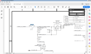
- F9700 (backlight fuse) as shown in the schematic, which can be looked up in the board view.
-
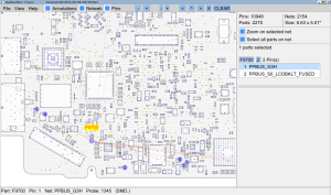
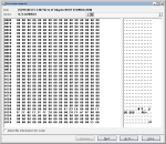
- OpenBoardView in use, showing what F9700 connects to, and where.
Power Supply
Before any device can perform any useful functions, it needs power. I reconnected the AC adapter and started to check the voltages around the DC input jack and its surrounding support circuitry. Since I was able to press the MacBook’s battery indicator and get some response when connected to power, I knew that the main input fuse was intact, and that the SMC (System Management Controller) chip was receiving power via the PP3V42_G3H rail and functional; the G3H (G3-Hot) designation means that the power rail is always on, even if the computer is otherwise turned off. I checked the voltage at the DC jack’s ADAPTER_SENSE line, which is normally at approximately 3.3 volts and uses the 1-Wire protocol to communicate with the power adapter and control the LED on the power adapter’s MagSafe plug. To my surprise, it was at a staggering 16 volts, which meant that something was shorting the DC input voltage (about 16.5 volts) onto a low-voltage communication line – no wonder there wasn’t any LED indicator when I plugged it in! A multimeter measurement found about 2 kOhms of resistance from the power line to the communication line. Thankfully the MacBook’s logic board features a MAX9940 1-Wire overvoltage protection chip, which is rated to protect against voltages as high as 30 volts. I scavenged another DC input connector from an older, dead MacBook which shared the same connector and pinout. After connecting this to the logic board, I found that I got a green LED upon connecting the AC adapter, and the CPU fan started spinning; this is a very good sign as this means the main power circuitry is intact. Measuring the CPU’s Vcore voltage revealed a voltage of about 0.8 volts, which is normal for a modern laptop CPU. With the “heart” of the computer checked out, it was time to focus on the area most affected by the water damage.
LCD & Backlight
Examining the backlight connector and its surrounding circuitry revealed significant damage to many components and the PCB itself. The power supply pins on the LCD connector showed a significant amount of corrosion, and I was concerned that the backlight’s output voltage (up to 52 volts!) could have made its way through all the corrosion residue and damaged critical data lines between the display and the graphics controller. I noticed the backlight fuse (F9700, a 3-amp 0603-size fuse) had gone more than just open-circuit – I couldn’t even find the fuse or its corresponding PCB pads initially! I then probed the LCD connector and found that the display’s 3.3-volt power lines were open-circuit; the corrosion had eaten through the traces between the connector and its decoupling capacitors nearby. Using a diode-mode measurement on the FPD-Link (often called LVDS) lines revealed that the connections were intact; there weren’t any anomalous readings or short-circuits on those lines, the DDC (Display Data Channel) lines, and the 3.3-volt power lines.
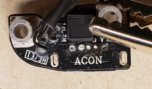
Due to the high voltages used to drive LED backlights, I had my suspicions on U9701 (a Texas Instruments LP8550 LED backlight driver). It’s a tiny ball-grid array (BGA) package, and attempts to clean the chip from its edges didn’t seem to do much. Its corrosion looked limited at first – only the feedback line’s probe point was lost – but I was sure the chip was on its last legs (or is it balls?).
Power Management
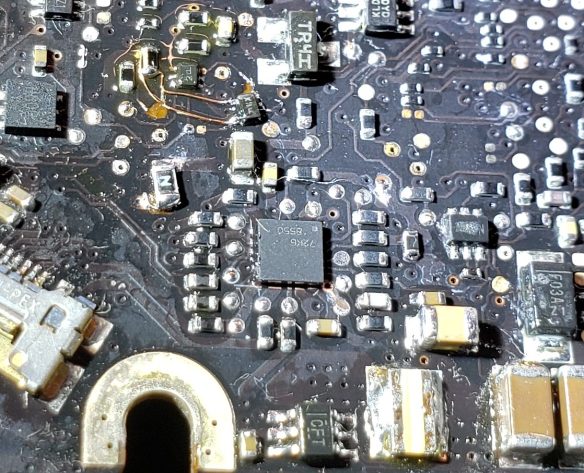
The LCD connector is in close proximity to the computer’s DC input and its “PPBUS_G3Hot” power rail, which is always on (even if the computer is otherwise turned off), which exacerbates any corrosion due to liquid damage due to its high voltage. Further examination revealed significant corrosion on the outside of the CPU’s high-side current sense resistor (R5400), and the current-measurement pins (pins 4 and 5) on U5400 (a Texas Instruments INA213 current-sense amplifier) were completely gone! Clearly there was no way to salvage that component.
There was significant damage to the SMC’s DC input voltage sense circuitry (“VD0R”), with pins 3 and 4 of Q5490 (an ON Semiconductor NTUD3169CZ complementary pair of N-channel and P-channel MOSFETs) being completely eroded away, much like U5400’s current-sense pins; this part of the circuit uses a P-channel MOSFET to switch on a resistive voltage divider, allowing the SMC to measure what the voltage is on its MagSafe input connector. Also, many of the probe points related to that circuit were also completely eroded, revealing dark pits instead of silver-plated copper pads.
FireWire
The FireWire circuit wasn’t spared from the carnage, either. Pins 3 and 4 on Q4262 (a Diodes Incorporated BSS8042DW complementary MOSFET pair) were also severely damaged; these pins are used to quickly disable the FireWire power output transistor (Q4260, an ON Semiconductor FDC638P P-channel MOSFET) in case of a “Late-VG event“. This occurs if the ground pins of the FireWire connector are mated too late when plugging in a device – this creates a dangerous overvoltage condition on the FireWire data lines, as up to 30 volts briefly find a return path through the data lines, risking damage to the device and host controller. I wasn’t as concerned with this circuit, as I don’t have any FireWire peripherals, and the circuit in its current state simply means the FireWire port will be unable to disconnect power if a bad cord is plugged in.
Thunderbolt
The area that had the least liquid damage was C3897, which belonged to U3890 (a Linear Technologies LT3957, a 15-volt boost converter for the MacBook’s T29 chip and Thunderbolt interface). All this area needed was a bit of corrosion cleanup.
USB Port
During the functionality tests, I noticed the metal casings of the USB port were getting very hot to the touch, and I nearly burned myself on U4600 (a Texas Instruments TPS2561, a dual-channel load switch with internal current limiting)! I found a short-to-ground problem on a power line on one of the USB ports, which explains the symptom listed on the note. I desoldered the chip, initially thinking the issue was in the chip itself, but the fault remained. I narrowed the problem down to C4695, a 10-microfarad ceramic capacitor that had short-circuited internally; this caused the TPS2561 to go into current-limiting mode, which turns the chip into a resistor and dissipate copious amounts of heat into the PCB, which made its way to the USB ports (and then my fingers – ouch).
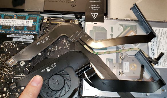
Hard Drive Cable
During the repair process, I was able to install Mac OS X Lion to a SATA SSD, but soon found the MacBook unable to recognize SSDs, despite hard disk drives showing up just fine! As it turns out, the A1278 is notorious for bad HDD cables, with even replacements failing within months of installation. This appeared to be caused by chronic frictional damage, as the cable is sandwiched between the hard drive and the MacBook’s rough aluminum casing – even regular use of the laptop was found to create hairline cracks in the cable. Thankfully replacements are relatively inexpensive, and a little bit of Kapton tape as a barrier against the casing was the “vaccine” against future cable failures.
-
- Replacement SATA cable on top. The PCB traces seem thicker and more robust than the original.
Repairs
With all of the problems written down, it was time to start fixing up the MacBook. Time to break out the hot air rework station, soldering iron, solder, magnet wire, and plenty of flux!
DC Input Jack
I desoldered the DC input jack, and found there was a lot of corrosion residue bridging the +16.5-volt power line to the ADAPTER_SENSE 1-Wire communication line.
-
- Black corrosion deposits under the MagSafe connector, causing a high-resistance short of the ADAPTER_SENSE data line to 16.5 volts.
-
- The PCB side of the corroded MagSafe connector. Note the loss of copper on the pads.
With some isopropyl alcohol and some scrubbing with a small brush, I was able to clean up the corrosion and resoldered the jack into place. A quick multimeter test found that there was no more 2 kOhms of resistance from the power to the data line, and I was able to get an LED indication when I plugged in the AC adapter, including an orange light that indicates the battery is charging.
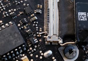
LCD Connector
I wanted to determine if the display was still functional, so I first focused my attention to the LCD connector, even if I had to eschew the LED backlight for a bit.
I ran a jumper wire from L9004 to pins 2 and 3 of the LCD connector; this belongs to PP3V3_LCDVDD_SW_F, which provides the 3.3-volt power to run the LCD panel except the backlight. After cleaning out the flux and corrosion on the logic board’s connector as well as the LCD cable, I was able to get an image on the display!
-
- Jumper from L9004 to pins 2 and 3 on J9000 backlight connector. Damage to Q4262 also visible.
-

- A “frontlit” MacBook LCD.
USB Port
With the faulty component identified, I replaced C4695 with an identically-rated 10-microfarad 6.3-volt X5R ceramic capacitor in an 0603-sized package. After replacing the capacitor, the USB port was fully functional again!
-
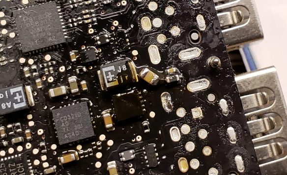
- Replaced C4695 USB output capacitor. 10 uF, 6.3 volt X5R, 0603 size.
Current-Sense Amplifier
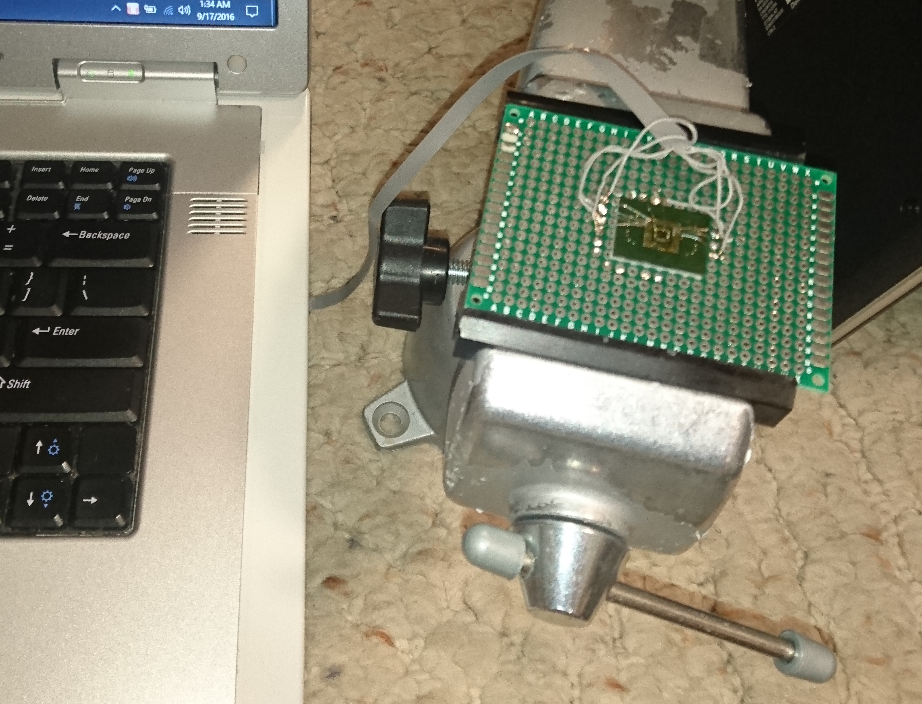
After ordering both the INA213 and LP8550 from Texas Instruments, it was only a few days before they arrived in the mail. I desoldered the dead chip from the logic board, cleaned up the pads with some flux and desoldering braid, and installed the new chip. Running Apple Service Diagnostic tools showed that the current-sensing circuit was working correctly.
DC Input Voltage Divider Switch
-
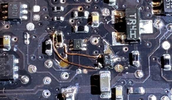
- Replaced PFET half of Q5490 (centre) with NTK3142P, bypassing lost traces/probe points. R5494 replaced with wire jumper, on left.
I didn’t want to buy another transistor pair for Q5490, so I replaced the P-channel half with an ON Semiconductor NTK3142P P-channel MOSFET that I salvaged from an older donor MacBook logic board. I scraped away some solder mask on one of the broken traces heading to the SMC’s voltage divider so I could solder the transistor’s drain terminal to it, and used magnet wire to connect the transistor’s gate and source to their corresponding locations across R5491. R5494, leading to PM_SUS_EN, was found to have a 0-ohm resistor that was open-circuit; this was easily bypassed with a wire jumper across the resistor’s original pads. After cleaning off the flux and performing continuity measurements, I measured the voltage at the SMC’s voltage divider resistors and got a valid voltage reading when I plugged in the AC adapter.
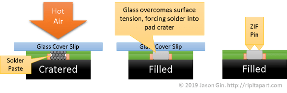
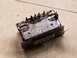
LED Backlight Driver
The LP8550 was up next for repair. I took a 2-amp 0603-sized fuse from a dead hard drive, and used some magnet wire to reattach it to the remnants of F9700, which was a 3-amp fuse originally; note that it’s far safer to use a fuse of a smaller rating instead of a larger one, should a circuit fault still exist.
Tracing the other lines to the LP8550 revealed that R9731 (leading to PPBUS_SW_LCDBKLT_PWR) was open-circuit at a via, which was easily bridged with some solder and magnet wire. R9010 (leading to PPBUS_SW_BKL) was open as well.
After reinstalling the fuse, I actually got the backlight working! However, upon a power cycle I heard a snap, saw a puff of smoke, and lost the original backlight chip. Chances are there was indeed some corrosion residue had caused 50-odd volts to end up on a more sensitive pin on the LP8550. I used an Xacto knife to lightly scratch an outline around the chip, then used copious amounts of flux and desoldered the dead chip with my hot air rework station; I also removed the fuse to help in further troubleshooting to ensure that there weren’t any short-circuits to ground on the backlight circuit. I cleaned up the area with leaded solder and some solder wick, and cleaned up the residual flux in anticipation of the new chip’s installation.
-
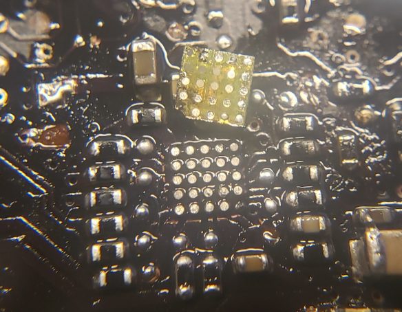
- The remnants of the original LP8550 (U9701). Note the damage to lowest-right ball on PCB, lowest-left on chip. F9700 temporarily removed.
-
- New LP8550 installed, with replacement fuse.
The chip was remarkably easy to install – just get the A1 ball lined up according to the board view, and heat the board to the right temperature. After thoroughly cleaning away the flux from the area, I turned on the MacBook… and let there be (back)light! I power-cycled the computer and the LED backlight remained functional! (And for the record, the fuse didn’t even blow during the entire ordeal.)
FireWire Late-VG Protection Circuit
I considered this issue to be a “WONTFIX“, as I had no use for FireWire connectivity (nor do I have the correct FireWire 800 cables anyway). If I want to sell this computer, I might install a P-channel MOSFET to replace Q4262 (see the LCD Connector section above) in a similar fashion to the DC input voltage-sensing circuitry.
UPDATE (February 26, 2020): Actually, several months ago I decided to finish things once and for all, so I replaced the damaged P-channel MOSFET circuitry. Do I have much use for FireWire? Not really, but it at least means I can experiment with it or something later on, if desired.
Testing
It takes a little bit of Google-Fu, but with the help of a BitTorrent client, I downloaded the disk images to create an Apple Service Diagnostic (ASD) drive. This is far more sophisticated than the built-in diagnostic when you boot the computer while holding down the D key. With ASD, one has the option to use a stripped-down version of Mac OS X – in a similar vein as WinPE – or a very lightweight UEFI (Universal Extensible Firmware Interface) environment that looks very much like Mac OS 9 and earlier.
-
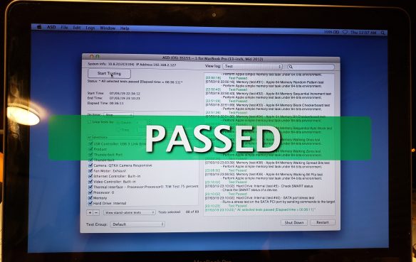
- LCD backlight restored; all tests passed in Apple Service Diagnostic!
It took over half an hour, but all the tests passed without a problem, since all the sensor readings were valid. My MacBook Pro has been restored to working order! I installed Mac OS X High Sierra to a 1TB SSD, and used Boot Camp to run Windows 10 Pro as the default operating system (what can I say, I like Windows 🙂 ). The Mac Precision Touchpad driver project makes the touchpad a pleasure to use, as the built-in Boot Camp driver provides a much less-comfortable experience.
Conclusion
Much like solving a puzzle, component-level troubleshooting of modern electronics is possible, but this is only feasible if the relevant documentation exists as a good reference point. One can do without them, but the act of reverse engineering isn’t easy if one only has a non-working device.
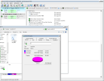
With the help of a schematic and board view (including the open-source software OpenBoardView), one can easily find what circuits a component belongs to, and where it goes. By following the connections, one can track down the problem(s) with the board, and hopefully save a device from an untimely end in the landfill or a recycling facility.
Right to Repair
This project is an example of why I believe in the right to repair. If I didn’t have (even unofficial) access to schematics, board views, and diagnostic software, I wouldn’t have been able to bring this dead MacBook Pro back to life. However, with a little bit of electronics troubleshooting knowledge and skill, I was delighted that I diverted a discarded dysfunctional device from a demise in the dumpster. In fact, this blog post was written from the MacBook I just repaired!