As seen on Hackaday!
TL;DR – The SanDisk High Endurance cards use SanDisk/Toshiba 3D TLC Flash. It took way, way more work than it should have to figure this out (thanks for nothing, SanDisk!).
In contrast, the SanDisk MAX Endurance uses the same 3D TLC in pMLC (pseudo-multi-level cell) mode.
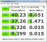
In a previous blog post, I took a look at SanDisk’s microSD cards that were aimed for use in write-intensive applications like dash cameras. In that post I took a look at its performance metrics, and speculated about what sort of NAND Flash memory is used inside. SanDisk doesn’t publish any detailed specifications about the cards’ internal workings, so that means I have no choice but to reverse-engineer the can of worms card myself.
The Help Desk That Couldn’t
In the hopes of uncovering more information, I sent an email to SanDisk’s support team asking about what type of NAND Flash they are using in their High Endurance lineup of cards, alongside endurance metrics like P/E (Program/Erase) cycle counts and total terabytes written (TBW). Unfortunately, the SanDisk support rep couldn’t provide a satisfactory answer to my questions, as they’re not able to provide any information that’s not listed in their public spec sheets. They said that all of their cards use MLC Flash, which I guess is correct if you call TLC Flash 3-bit MLC (which Samsung does).
Dear Jason,
Thank you for contacting SanDisk® Global customer care. We really appreciate you being a part of our SanDisk® family.
I understand that you wish to know more about the SanDisk® High Endurance video monitoring card, as such please allow me to inform you that all our SanDisk® memory cards uses Multi level cell technology (MLC) flash. However, the read/write cycles for the flash memory is not published nor documented only the read and write speed in published as such they are 100 MB/S & 40 MB/s. The 64 GB card can record Full HD video up to 10,000 hours. To know more about the card you may refer to the link below:
SANDISK HIGH ENDURANCE VIDEO MONITORING microSD CARD
Best regards,
Allan B.
SanDisk® Global Customer Care
I’ll give them a silver star that says “You Tried” at least.
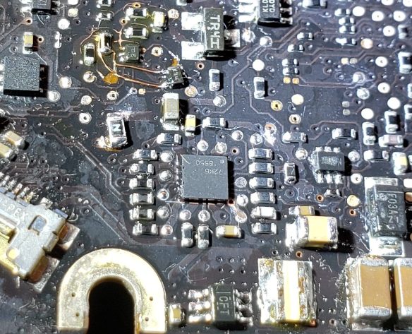
Anatomy of an SD Card
While (micro)SD cards feel like a solid monolithic piece of technology, they’re made up of multiple different chips, each performing a different role. A basic SD card will have a controller that manages the NAND Flash chips and communicates with the host (PC, camera, etc.), and the NAND Flash itself (made up of 1 or more Flash dies). Bunnie Huang’s blog, Bunnie Studios, has an excellent article on the internals of SD cards, including counterfeits and how they’re made – check it out here.

Block diagram of a typical SD card.
MicroSD cards often (but not always!) include test pads, used to program/test the NAND Flash during manufacture. These can be exploited in the case of data recovery, or to reuse microSD cards that have a defective controller or firmware by turning the card into a piece of raw NAND Flash – check out Gough Lui’s adventures here. Note that there is no set standard for these test pads (even for the same manufacturer!), but there are common patterns for some manufacturers like SanDisk that make reverse-engineering easier.
Crouching Controller, Hidden Test Pads
microSD cards fall into a category of “monolithic” Flash devices, as they combine a controller and raw NAND Flash memory into a single, inseparable package. Many manufacturers break out the Flash’s data bus onto hidden (and nearly completely undocumented) test pads, which some other memory card and USB drive manufacturers take advantage of to make cheap storage products using failed parts; the controller can simply be electrically disabled and the Flash is then used as if it were a regular chip.
In the case of SanDisk cards, there is very limited information on their cards’ test pad pinouts. Each generation has slight differences, but the layout is mostly the same. These differences can be fatal, as the power and ground connections are sometimes reversed (this spells instant death for a chip if its power polarity is mixed up!).
CORRECTION (July 22, 2020): Upon further review, I might have accidentally created a discrepancy between the leaked pinouts online, versus my own documentation in terms of power polarity; see the “Test Pad Pinout” section.
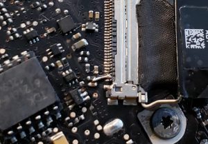
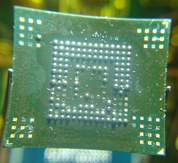
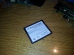
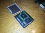
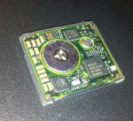
My card (and many of their higher-end cards – that is, not their Ultra lineup) features test pads that aren’t covered by solder mask, but are instead covered by some sort of screen-printed epoxy with a laser-etched serial number on top. With a bit of heat and some scraping, I was able to remove the (very brittle) coating on top of the test pads; this also removed the serial number which I believe is an anti-tamper measure by SanDisk.
-

- Epoxy coating over test pads
-

- Test pads exposed
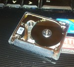
After cleaning off any last traces of the epoxy coating, I was greeted with the familiar SanDisk test pad layout, plus a few extra on the bottom.
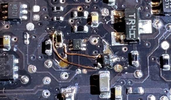
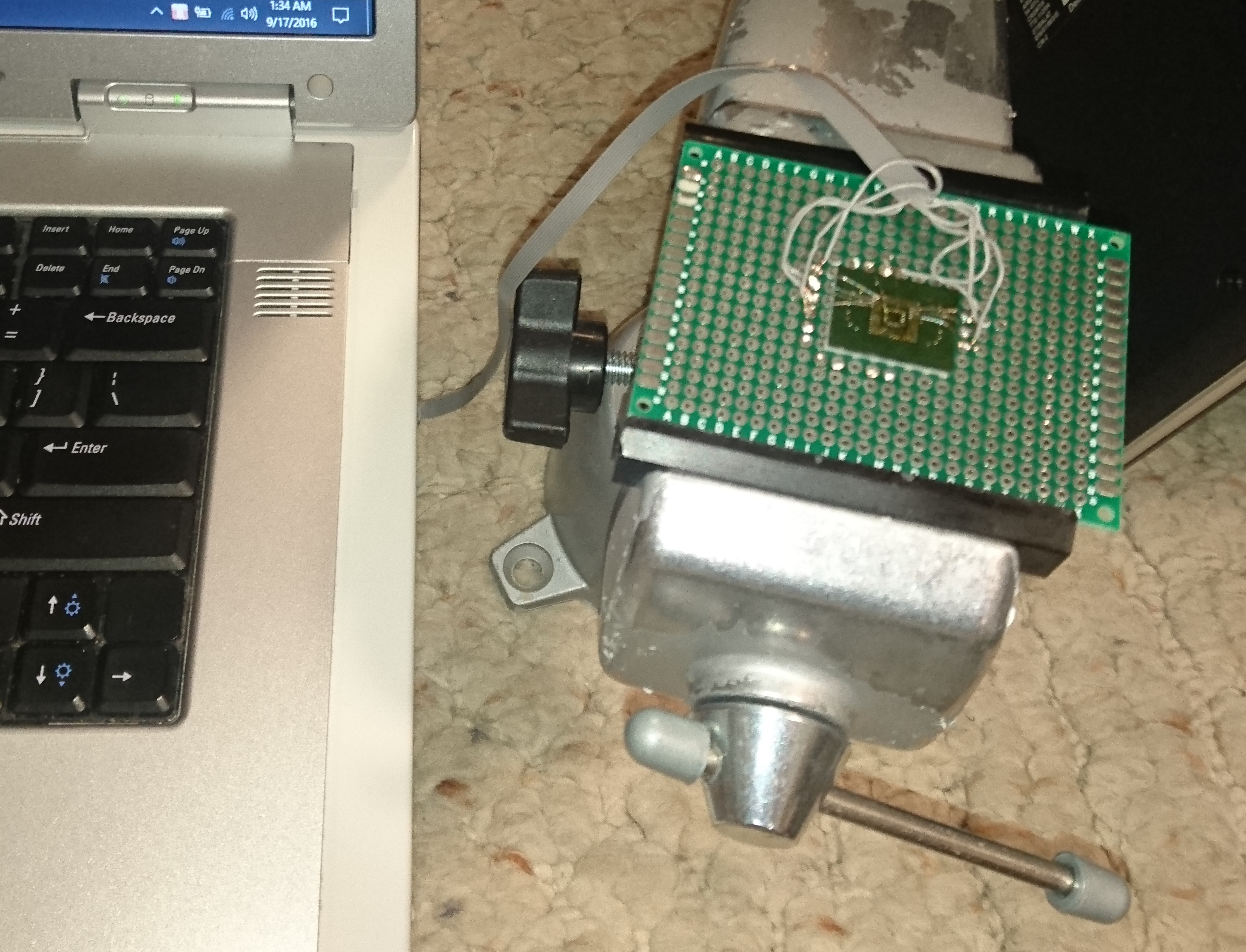
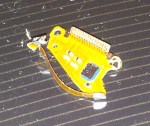
Building the Breakout Board
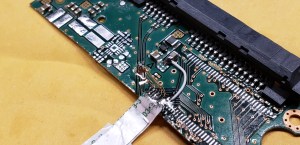
The breakout board is relatively simple in concept: for each test pad, bring out a wire that goes to a bigger test point for easier access, and wire up the normal SD bus to an SD connector to let the controller do its work with twiddling the NAND Flash bus. Given how small each test pad is (and how many), things get a bit… messy.
-

- Breakout board assembled.
-

- Closeup of card breakout.
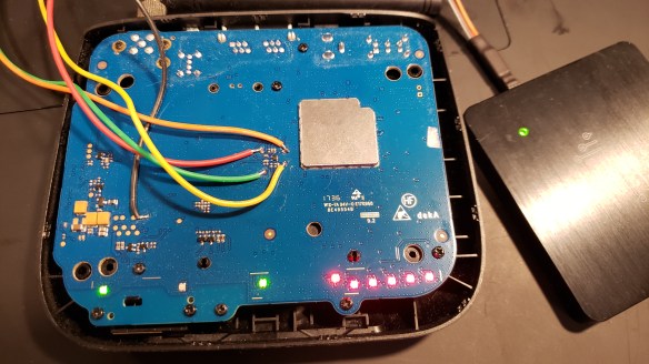
I started by using double-side foam adhesive tape to secure the SD card to a piece of perfboard. I then tinned all of the pads and soldered a small 1uF ceramic capacitor across the card’s power (Vcc) and ground (GND) test pads. Using 40-gauge (0.1 mm, or 4-thousandths of an inch!) magnet wire, I mapped each test pad to its corresponding machine-pin socket on the perfboard. Including the extra test pads, that’s a total of 28 tiny wires!
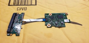
For the SD connector side of things, I used a flex cable for the XTC 2 Clip (a tool used to service HTC Android devices), as it acted as a flexible “remote SD card” and broke out the signals to a small ribbon cable. I encased the flex cable with copper tape to act as a shield against electrical noise and to provide physical reinforcement, and soldered the tape to the outer pads on the perfboard for reinforcement. The ribbon cable end was then tinned and each SD card’s pin was wired up with magnet wire. The power lines were then broken out to an LED and resistor to indicate when the card was receiving power.
Bus Analysis
With all of the test pads broken out to an array of test pins, it was time to make sense of what pins are responsible for accessing the NAND Flash inside the card.
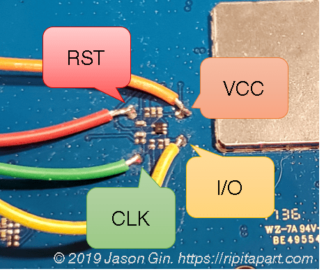
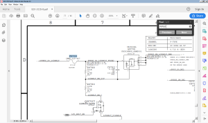
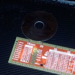
Test Pad Pinout

Diagram of the test pads on SanDisk’s High Endurance microSD card. (click to enlarge)
The overall test pad pinout was the same for other microSD cards from SanDisk, but there were some differences, primarily regarding the layout of the power pads; notably, the main power pins are backwards! This can destroy the card if you’re not careful when applying power.
CORRECTION (July 22, 2020): I might actually have just gotten my own documentation mixed up in terms of the power and ground test pads. Regardless, one should always be careful to ensure the correct power polarity is sent to a device.
I used my DSLogic Plus logic analyzer to analyze the signals on all of the pins. Since the data pinout was previously discovered, the hard part of figuring out what each line represented (data bus, control, address, command, write-protect, ready/busy status) was already done for me. However, not all of the lines were immediately evident as the pinouts I found online only included the bare minimum of lines to make the NAND Flash accessible, with one exception being a control line that places the controller into a reset state and releases its control of the data lines (this will be important later on).
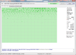
By sniffing the data bus at the DSLogic’s maximum speed (and using its 32 MB onboard buffer RAM), I was able to get a clear snapshot of the commands being sent to the NAND Flash from the controller during initialization.
Bus Sniffing & NAND I/O 101 (writing commands, address, reading data)
In particular, I was looking for two commands: RESET (0xFF), and READ ID (0x90). When looking for a command sequence, it’s important to know how and when the data and control lines change. I will try to explain it step-by-step, but if you’re interested there is an introductory white paper by Micron that explains all of the fundamentals of NAND Flash with much more information about how NAND Flash works.
-

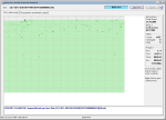
- Logic analyzer trace of RESET command. Dotted line indicates where the write and reset occurs.
-

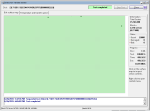
- Logic analyzer trace of READ ID command. Dotted lines indicate where read/writes occur.
When a RESET command is sent to the NAND Flash, first the /CE (Chip Select, Active Low) line is pulled low. Then the CLE (Command Latch Enable) line is pulled high; the data bus is set to its intended value of 0xFF (all binary ones); then the /WE (Write Enable, Active Low) line is pulsed from high to low, then back to high again (the data bus’ contents are committed to the chip when the /WE line goes from low to high, known as a “rising edge”); the CLE line is pulled back low to return to its normal state. The Flash chip will then pull its R/B (Ready/Busy Status) line low to indicate it is busy resetting itself, then releases the line back to its high state when it’s finished.
The READ ID command works similarly, except after writing the command with 0x90 (binary 1001 0000) on the data bus, it then pulls the ALE (Address Latch Enable) line high instead of CLE, and writes 0x00 (all binary zeroes) by pulsing the /WE line low. The chip transfers its internally programmed NAND Flash ID into its internal read register, and the data is read out from the device on each rising edge of the /RE (Read Enable, Active Low) line; for most devices this is 4 to 8 bytes of data.
NAND Flash ID
For each NAND Flash device, it has a (mostly) unique ID that identifies the manufacturer, and other functional data that is defined by that manufacturer; in other words, only the manufacturer ID, assigned by the JEDEC Technology Association, is well-defined.
The first byte represents the Flash manufacturer, and the rest (2 to 6 bytes) define the device’s characteristics, as set out by the manufacturer themselves. Most NAND vendors are very tight-lipped when it comes to datasheets, and SanDisk (and by extension, Toshiba/Kioxia) maintain very strict control, save for some slightly outdated leaked Toshiba datasheets. Because the two aforementioned companies share their NAND fabrication facilities, we can reasonably presume the data structures in the vendor-defined bytes can be referenced against each other.
In the case of the SanDisk High Endurance 128GB card, it has a NAND Flash ID of 0x45 48 9A B3 7E 72 0D 0E. Some of these values can be compared against a Toshiba datasheet:
| Byte Value (Hex) | Description/Interpretation |
|---|---|
| 45 |
|
| 48 |
|
| 9A |
|
| B3 |
|
| 7E |
|
| 72 |
|
| 0D |
|
| 0E |
|
Although not all byte values could be conclusively determined, I was able to determine that the SanDisk High Endurance cards use BiCS3 3D TLC NAND Flash, but at least it is 3D NAND which improves endurance dramatically compared to traditional/planar NAND. Unfortunately, from this information alone, I cannot determine whether the card’s controller takes advantage of any SLC caching mechanisms for write operations.
The chip’s process geometry was determined by looking up the first four bytes of the Flash ID, and cross-referencing it to a line from a configuration file in Silicon Motion’s mass production tools for their SM3271 USB Flash drive controller, and their SM2258XT DRAM-less SSD controller. These tools revealed supposed part numbers of SDTNAIAMA-256G and SDUNBIEMM-32G respectively, but I don’t think this is accurate for the specific Flash configuration in this card.
External Control
I wanted to make sure that I was getting the correct ID from the NAND Flash, so I rigged up a Texas Instruments MSP430FR2433 development board and wrote some (very) rudimentary code to send the required RESET and READ ID commands, and attempt to extract any extra data from the chip’s hidden JEDEC Parameter Page along the way.
My first roadblock was that the MSP430 would reset every time it attempted to send the RESET command, suggesting that too much current was being drawn from the MSP430 board’s limited power supply. This can occur during bus contention, where two devices “fight” each other when trying to set a certain digital line both high and low at the same time. I was unsure what was going on, since publicly-available information didn’t mention how to disable the card’s built-in controller (doing so would cause it to tri-state the lines, effectively “letting go” of the NAND bus and allowing another device to take control).
I figured out that the A1 test pad (see diagram) was the controller’s reset line (pulsing this line low while the card was running forced my card reader to power-cycle it), and by holding the line low, the controller would release its control of the NAND Flash bus entirely. After this, my microcontroller code was able to read the Flash ID correctly and consistently.

Reading out the card’s Flash ID with my own microcontroller code.
JEDEC Parameter Page… or at least what SanDisk made of it!
The JEDEC Parameter Page, if present, contains detailed information on a Flash chip’s characteristics with far greater detail than the NAND Flash ID – and it’s well-standardized so parsing it would be far easier. However, it turns out that SanDisk decided to ignore the standard format, and decided to use their own proprietary Parameter Page format! Normally the page starts with the ASCII string “JEDEC”, but I got a repeating string of “SNDK” (corresponding with their stock symbol) with other data that didn’t correspond to anything like the JEDEC specification! Oh well, it was worth a try.
I collected the data with the same Arduino sketch as shown above, and pulled 1,536 bytes’ worth of data; I wrote a quick program on Ideone to provide a nicely-formatted hex dump of the first 512 bytes of the Parameter Page data:
Offset 00:01:02:03:04:05:06:07:08:09:0A:0B:0C:0D:0E:0F 0123456789ABCDEF
------ --+--+--+--+--+--+--+--+--+--+--+--+--+--+--+-- ----------------
0x0000 53 4E 44 4B 53 4E 44 4B 53 4E 44 4B 53 4E 44 4B SNDKSNDKSNDKSNDK
0x0010 53 4E 44 4B 53 4E 44 4B 53 4E 44 4B 53 4E 44 4B SNDKSNDKSNDKSNDK
0x0020 08 08 00 08 06 20 00 02 01 48 9A B3 00 05 08 41 ..... ...H.....A
0x0030 48 63 6A 08 08 00 08 06 20 00 02 01 48 9A B3 00 Hcj..... ...H...
0x0040 05 08 41 48 63 6A 08 08 00 08 06 20 00 02 01 48 ..AHcj..... ...H
0x0050 9A B3 00 05 08 41 48 63 6A 08 08 00 08 06 20 00 .....AHcj..... .
0x0060 02 01 48 9A B3 00 05 08 41 48 63 6A 08 08 00 08 ..H.....AHcj....
0x0070 06 20 00 02 01 48 9A B3 00 05 08 41 48 63 6A 08 . ...H.....AHcj.
0x0080 08 00 08 06 20 00 02 01 48 9A B3 00 05 08 41 48 .... ...H.....AH
0x0090 63 6A 08 08 00 08 06 20 00 02 01 48 9A B3 00 05 cj..... ...H....
0x00A0 08 41 48 63 6A 08 08 00 08 06 20 00 02 01 48 9A .AHcj..... ...H.
0x00B0 B3 00 05 08 41 48 63 6A 08 08 00 08 06 20 00 02 ....AHcj..... ..
0x00C0 01 48 9A B3 00 05 08 41 48 63 6A 08 08 00 08 06 .H.....AHcj.....
0x00D0 20 00 02 01 48 9A B3 00 05 08 41 48 63 6A 08 08  ...H.....AHcj..
0x00E0 00 08 06 20 00 02 01 48 9A B3 00 05 08 41 48 63 ... ...H.....AHc
0x00F0 6A 08 08 00 08 06 20 00 02 01 48 9A B3 00 05 08 j..... ...H.....
0x0100 41 48 63 6A 08 08 00 08 06 20 00 02 01 48 9A B3 AHcj..... ...H..
0x0110 00 05 08 41 48 63 6A 08 08 00 08 06 20 00 02 01 ...AHcj..... ...
0x0120 48 9A B3 00 05 08 41 48 63 6A 08 08 00 08 06 20 H.....AHcj.....
0x0130 00 02 01 48 9A B3 00 05 08 41 48 63 6A 08 08 00 ...H.....AHcj...
0x0140 08 06 20 00 02 01 48 9A B3 00 05 08 41 48 63 6A .. ...H.....AHcj
0x0150 08 08 00 08 06 20 00 02 01 48 9A B3 00 05 08 41 ..... ...H.....A
0x0160 48 63 6A 08 08 00 08 06 20 00 02 01 48 9A B3 00 Hcj..... ...H...
0x0170 05 08 41 48 63 6A 08 08 00 08 06 20 00 02 01 48 ..AHcj..... ...H
0x0180 9A B3 00 05 08 41 48 63 6A 08 08 00 08 06 20 00 .....AHcj..... .
0x0190 02 01 48 9A B3 00 05 08 41 48 63 6A 08 08 00 08 ..H.....AHcj....
0x01A0 06 20 00 02 01 48 9A B3 00 05 08 41 48 63 6A 08 . ...H.....AHcj.
0x01B0 08 00 08 06 20 00 02 01 48 9A B3 00 05 08 41 48 .... ...H.....AH
0x01C0 63 6A 08 08 00 08 06 20 00 02 01 48 9A B3 00 05 cj..... ...H....
0x01D0 08 41 48 63 6A 08 08 00 08 06 20 00 02 01 48 9A .AHcj..... ...H.
0x01E0 B3 00 05 08 41 48 63 6A 08 08 00 08 06 20 00 02 ....AHcj..... ..
0x01F0 01 48 9A B3 00 05 08 41 48 63 6A 08 08 00 08 06 .H.....AHcj.....
Further analysis with my DSLogic showed that the controller itself requests a total of 4,128 bytes (4 kiB + 32 bytes) of Parameter Page data, which is filled with the same repeating data as shown above.
Reset Quirks
When looking at the logic analyzer data, I noticed that the controller sends the READ ID command twice, but the first time it does so without resetting the Flash (which should normally be done as soon as the chip is powered up!). The data that the Flash returned was… strange to say the least.
| Byte Value (Hex) | Interpreted Value |
|---|---|
| 98 |
|
| 00 |
|
| 90 |
|
| 93 |
|
| 76 |
|
| 72 |
|
This confused me initially when I was trying to find the ID from the logic capture alone; after talking to a contact who has experience in NAND Flash data recovery, they said this is expected for SanDisk devices, which make liberal use of vendor-proprietary commands and data structures. If the fourth byte is to be believed, it says the block size is 4 megabytes, which I think is plausible for a modern Flash device. The rest of the information doesn’t really make any sense to me apart from the first byte indicating the chip is made by Toshiba.
Conclusion
I shouldn’t have to go this far in hardware reverse-engineering to just ask a simple question of what Flash SanDisk used in their high-endurance card. You’d think they would be proud to say they use 3D NAND for higher endurance and reliability, but I guess not!
Downloads
For those that are interested, I’ve included the logic captures of the card’s activity shortly after power-up. I’ve also included the (very crude) Arduino sketch that I used to read the NAND ID and Parameter Page data manually: