TL;DR: XTAR’s new lithium-ion AA and AAA batteries offer a decent alternative to Ni-MH rechargeables if weight and/or output voltage is a concern, but only for low- and medium-drain applications. You can charge them directly with 5V if you don’t have a dedicated charger on hand. Their new L8 charger works for their Li-ion 1.5V batteries and third-party Ni-MH cells alike.
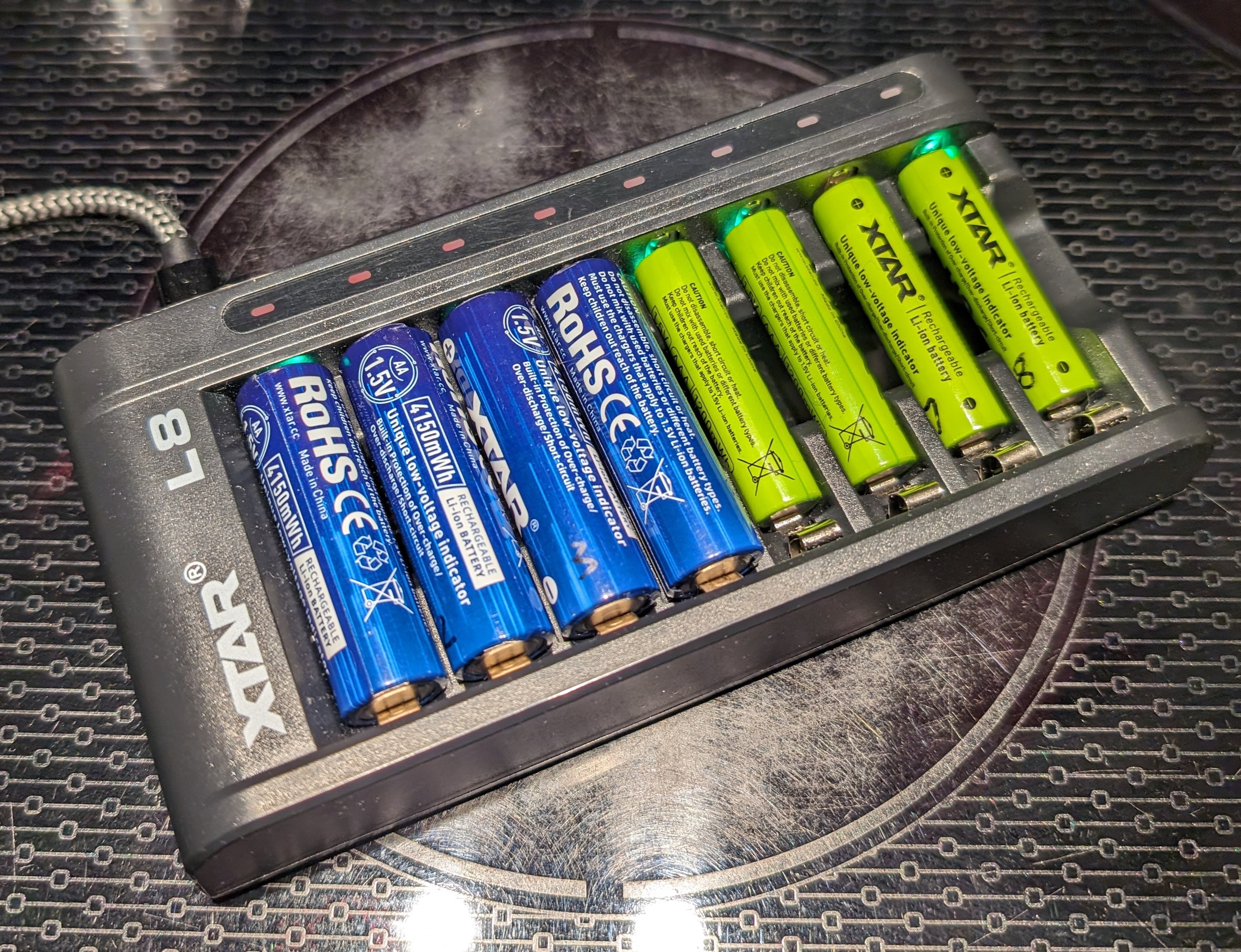
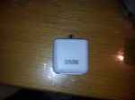
XTAR’s 4150mWh AA, and 1200mWh AAA Li-ion batteries in an XTAR L8 USB-C charger.
Lithium-ion AA and AAA batteries have been around for several years (see this review of the Kentli PH5 I made several years ago), but that doesn’t mean they haven’t made progress in energy density. Last summer, XTAR offered me a bundle of their latest and highest-capacity AA and AAA Li-ion batteries to try out, alongside their latest L8 multi-chemistry 8-bay charger. After several months of testing, I have collected enough data on which to base my review upon.
FULL DISCLOSURE: XTAR provided these batteries and corresponding charger to me at no charge for an independent review. They had no editorial control over this review, I have not been compensated monetarily, and all opinions expressed in this review are my own.
Introduction
XTAR is no stranger to the world of lithium-ion rechargeable batteries, and their new Li-ion 1.5V AA and AAA batteries offer an incremental improvement to their previous offerings, increasing their AA batteries from 3.3 watt-hours to 4.15 watt-hours of energy, and their 1.2 watt-hour AAA batteries enjoy a small performance boost from 1.5 amps to 1.6 amps of maximum continuous discharge current.
Like all Li-ion 1.5V batteries that use a DC-DC converter internally to regulate the nominal 3.7 volts from the internal cell down to 1.5 volts, XTAR’s AA/AAA batteries feature a flat discharge profile irrespective of load current and state of charge; their better offerings will even reduce their output voltage from 1.5 to 1.1 volts when the batteries near empty, helping to signal to the device they’re installed in that a recharge will soon be necessary; without this feature, a powered device will “think” it’s perpetually at 100% charge until it suddenly turns off.
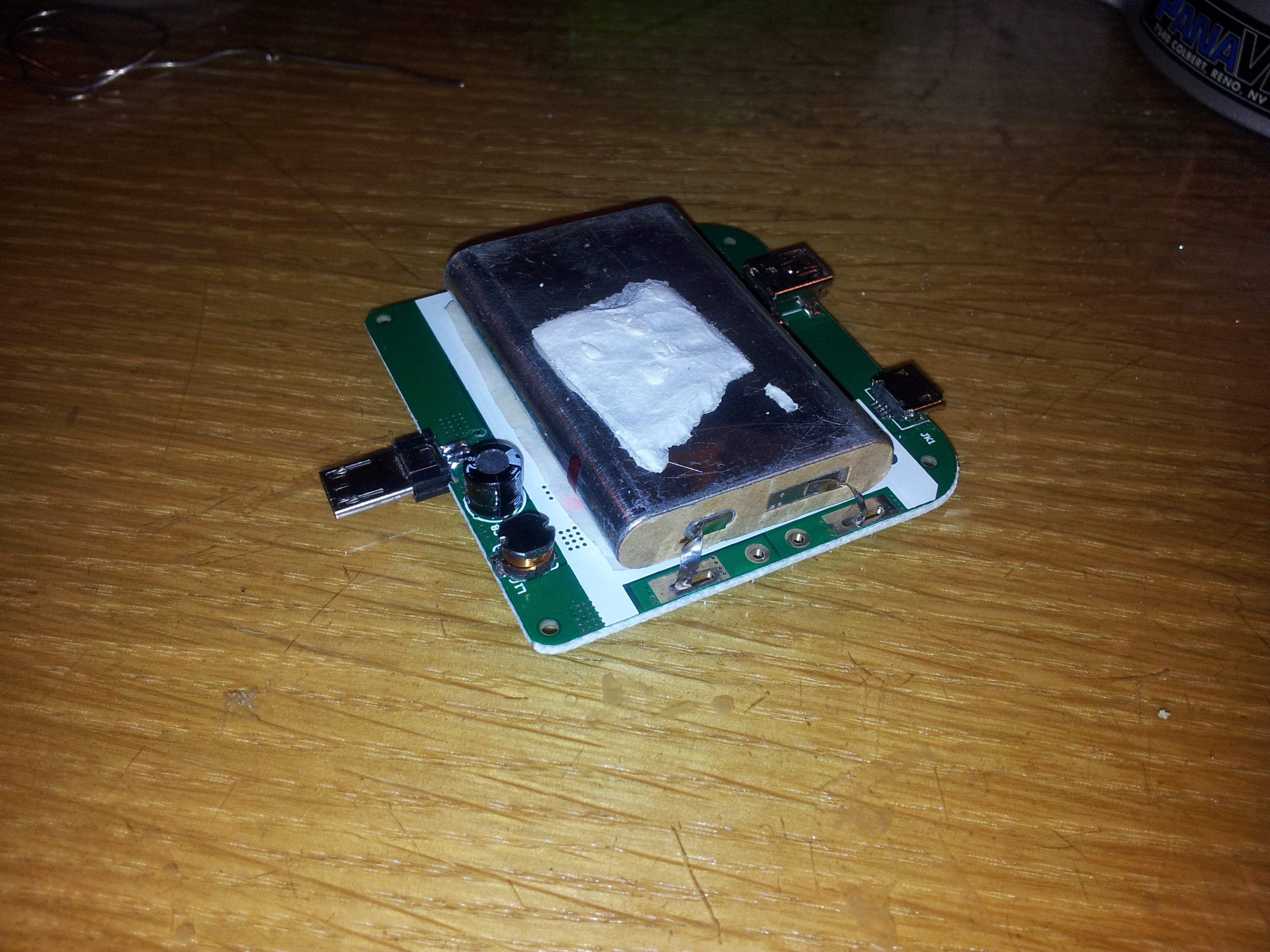
Some Li-ion 1.5V batteries include charge regulation circuitry internally, which makes charging them easier since you can provide 5 volts from USB power to directly charge them. Some have a (micro-)USB or USB-C port to do this, but at the expense of battery capacity due to the physical space they take up. XTAR gets around this by including a linear charge controller in the positive end cap of the battery, but allows charging by feeding 5 volts into the same terminals used to discharge them. This makes DIY charging of their batteries easy, if one doesn’t want to spend extra for a dedicated charger. That said, the XTAR L8 charger offers multi-chemistry support, charging their Li-ion AA/AAAs as well as your existing Ni-MH cells. You don’t even need to group them by chemistry, as each charge bay is controlled independently – mix your cells to your heart’s content (just not in your device!). If you’ve already converted most of your USB charging gear to USB-C, you’re in luck – the L8 not only supports USB-C adapters with the correct 5.1k pulldown resistors, it supports requesting higher voltages (specifically, 9 volts) using Quick Charge 2.0 over the data pins for faster charge times (something I was unable to quantify since I don’t have enough test equipment on hand).
Battery Tests
For my discharge tests, I used my SkyRC MC3000 multi-chemistry battery analyzer, which was calibrated against my Keysight U1253B multimeter for both voltage and current measurements. Charging the batteries was performed using the L8 charger that XTAR provided me, as the MC3000 doesn’t support charging batteries with integrated charge regulation circuitry. Thermal performance was measured using an Inifiray P2 Pro thermal camera. The results of four cells were averaged together to get the data shown below.
I included tests of Ikea Ladda 2450mAh Ni-MH AA batteries as a means of comparing the performance of XTAR’s Li-ion technology against existing Ni-MH batteries, with the Ladda effectively being a rebrand of Panasonic’s Eneloop low-self-discharge Ni-MH battery.
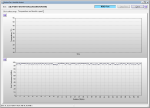
AA Capacity vs. Load
Testing the battery capacities with varying load currents revealed a “humped” curve reminiscent of my PH5 review; that is, there is a “sweet spot” where the extracted capacity is highest, rather than a simple downward slope for batteries that don’t use an internal DC-DC converter.

Chart showing the XTAR 4150mWh Li-ion AA’s capacity at different load currents.
The AA battery showed a peak of 2353mAh at 500mA, which might sound like it’s just under the Ladda’s capacity, but things change once we compare the amount of energy that each battery delivers.
XTAR 4150mWh Li-ion AA vs. Ikea Ladda 2450mAh Ni-MH AA

Chart comparing extracted energy from XTAR 4150mWh Li-ion AA vs. Ikea Ladda 2450mAh Ni-MH AA.
For these low to moderate loads, the XTAR AA comes out on top, mainly helped by its higher output voltage. This trend only holds true for the load range that the XTAR battery supports, though. Once you need a battery that can support heavier loads, then a high-drain capable Ni-MH battery is your only real option (but given its capacity-vs-load characteristic, it should provide more consistent performance irrespective of load current).
Now, in terms of the above data… I did have to smooth some numbers due to missing energy values, thanks to a bad data collection setup for some earlier data runs; to be more precise, I multiplied the capacity values with a nominal voltage to get the outputted energy values. However, the data trend itself remains the same.
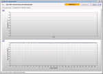
AAA Capacity vs. Load
The AAA batteries have a similar curve to the AAs, but peak at a lower discharge rate relative to its rated maximum discharge current. I didn’t have an equivalent AAA Ni-MH to test against.

Chart showing the XTAR 1200mWh AAA Li-ion battery’s capacity versus load current.

Chart showing the XTAR 1200mWh AAA Li-ion battery’s energy versus load current.
The equivalent nominal voltage is different for the AAA as it decreases to its 1.1V low-battery threshold much later than the AA does. However, its peak energy percentage is also slightly higher than the AA’s but both are in the mid-80% range.
Thermal Performance

Thermal capture of the XTAR 4150mWh AA Li-ion battery at maximum load.
One potential concern I have with the batteries is just how hot the regulator circuitry at the positive end gets when under heavy loads. While the AA battery is rated for 2 amps of continuous discharge current, the positive end of the battery reached upwards of 80 or 90 degrees Celsius, hot enough to distort the plastic label from the sustained heat. This ultimately isn’t unique to XTAR’s offerings (the Kentli PH5 I previously tested ran into the same issues at high loads), but is still something to be aware of when using these batteries in high-drain devices, especially ones that place a constant load on the battery. The AAAs aren’t quite as affected but still reached temperatures of almost 60 degrees Celsius at maximum rated load.

Thermal capture of XTAR L8 while charging four Ikea Ladda 2450mAh Ni-MH AAs, and four XTAR 4.15Wh Li-ion AAs. Note the heat generated at the positive terminal.
In terms of charging, the thermal issue remains but is much smaller. Heating of the positive end circuitry is largely unavoidable due to the use of a linear charge controller (but can you really expect to fit a switched-mode charger in the end cap of an AA/AAA battery?), with peak temperatures just under 50 degrees Celsius. This isn’t terribly hot compared to the peak temperature of a Ni-MH battery near the end of its charge cycle, which in the above image was about 40 degrees Celsius at the time of capture.
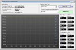
Charger Test (Ni-MH Charging)
I was curious as to how the L8 handles Ni-MH charging, so I captured the voltage and currents going into an Ikea Ladda 2450mAh cell with some jerry-rigged AA battery adapters and an AVHzY CT-3 USB meter.

Chart showing the voltage/current of the XTAR L8 while charging an AA Ni-MH cell.
The L8 charges at about 480mA but takes a small pause every 2 seconds to sample the cell’s voltage. Although I can’t say for certain, a zoomed-out look at the test data suggests that the L8 is uses the -dV/dt (voltage sag over time) method to determine when the cell is fully charged.
Conclusion
Overall, I’m quite satisfied with the batteries and charger. While the idea of sticking DC-DC converters inside a small battery case comes with limitations, it can still offer performance benefits for many applications.
Battery Pros
- Higher output voltage than Ni-MH
- Higher energy density than Ni-MH (within specified current range)
- Low-voltage feature drops the output from 1.5 to 1.1 volts when battery runs low
- Integrated charge circuitry allows batteries to charge directly from 5 volt power (DIY charging is easy)
- Lack of USB charge port means no space lost to a USB port (therefore, more battery capacity)
Battery Cons
- Integrated DC-DC converter limits efficiency
- Heat generation at high loads due to DC-DC converter when discharging, and linear charge regulator when charging
- Lower maximum discharge current compared to Ni-MH