Recovering the SIM card PIN from the ZTE WF721 cellular home phone

As seen on Hackaday!

TL;DR – If you have a ZTE WF721 that’s PIN-locked your SIM card, try 2376.

Recently I picked up a used Samsung Galaxy Core LTE smartphone from a relative after they upgraded to an iPhone. As the Core LTE is a low-end smartphone, I suspected that the phone was SIM locked to its original carrier (Virgin Mobile), but in order to test this I needed a different SIM card. My personal phone was on the same carrier, so I wasn’t able to use that to test it.

However, the previous summer I picked up a ZTE WF721 cellular home phone base station (that is, it’s a voice-only cell phone that a landline phone plugs into), which came with a Telus SIM card. The issue is that the WF721 sets a SIM card PIN to essentially “lock” the card to the base station, and it wasn’t the default 1234 PIN; brute-forcing a SIM card is not possible as you get 3-5 attempts before the card needs to be unblocked using a PUK (PIN Unblock Key), failing that, the card is permanently rendered unusable. I decided to take the base station apart, and use my knowledge in electronics and previous research into smart cards to see if I could recover the PIN.

(Yes, I went through all this work instead of just buying a prepaid SIM card from the dollar store. I’m weird like that.)

Test Pads & Signals

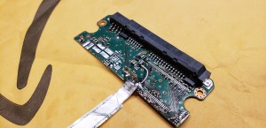
After a bit of disassembly work involving removing screws hidden under rubber non-slip feet and a lot of spudgering open plastic clips, I got access to the four test pads that connect to the SIM card, accessible on the opposite side of the PCB from the SIM card socket.

ZTE WF721 Opened

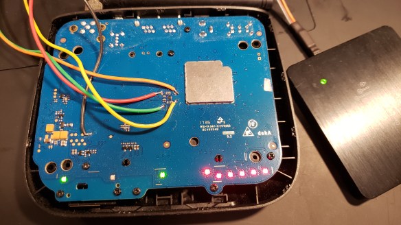
The ZTE WF721 opened, with test pads broken out and connected to DSLogic for reverse engineering.

An ISO 7816-compliant smart card (and a SIM card is one) require 5 different lines to work: Vcc (power), ground, clock, I/O (data), and reset. The I/O is an asynchronous half-duplex UART-type interface, whose baud rate is determined by the card’s characteristics and the clock frequency that it is given by the reader (in this case, the WF721). The details of how the interface work can be obtained for free in their TS 102 221 specification from the ETSI (European Telecommunications Standards Institute).

ZTE WF721 SIM Card Test Pads

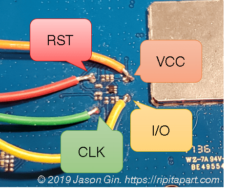
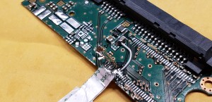
The test pads that connect to the WF721’s SIM card socket.

I then soldered the ground wire to a free test pad elsewhere on the board, whereas the four other wires were soldered to the test pads near the SIM card socket. I then connected these wires to a pin header and plugged it into my DSLogic Plus logic analyzer. I analyzed the logic captures after turning the WF721 on and allowing it to initialize the SIM card and attempt to connect to the cellular network (the service to it has been disconnected so it doesn’t actually succeed).

Command Analysis

After looking at the raw logic capture, there was a lot that I had to sift through. I needed to create a custom setting for the UART decoder as the serial output isn’t your traditional “9600-8-N-1” setting. Rather, the interface uses 8 data bits, even parity, and 2 stop bits. The baud rate is determined by a parameter in the card’s initial identification, the ATR (Answer to Reset). I parsed the card’s ATR that I previously captured on the PC using the SpringCard PC/SC Diagnostic tool using Ludovic Rousseau’s online tool, I determined I needed to use a baud rate of 250 kbit/s, since the card was being fed a 4 MHz clock.

T=0 Smart Card Command (APDU) Structure

The smart card communicates to and from the host through APDUs (Application Protocol Data Units). The command header for a T=0 smart card (character-based I/O, which most cards use) is made up of 5 bytes: class, instruction, 2 parameter bytes and a length/3rd parameter byte. To acknowledge the command, the card sends the instruction byte back to the reader and the data is transferred to/from the card, depending on the command used. The card then sends two status bytes that indicate whether the command is successful; if it is, the response is 0x9000. A graphical representation of this process can be seen in the next section.

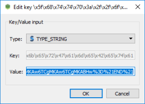
VERIFY PIN Command Decoding

The raw data structure of a SIM card's VERIFY PIN command. Each part of the flow is labeled for ease of understanding.

The raw data structure of a SIM card’s VERIFY PIN command. Each part of the flow is labeled for ease of understanding (click image to see full size).

The command I’m looking for is 0x20 (VERIFY PIN), and I had to sift through the command flow in the logic analyzer until I found it. After a lot of preceding commands, I found the command I was looking for, and I found the PIN… and it’s in plaintext! As it turns out, it is sent as an ASCII string, but it’s not null terminated like a regular string. Instead, the data is always 8 bytes (allowing up to an 8-digit PIN), but a PIN shorter than 8 digits will have the end bytes padded with 0xFF (all binary ones). It was easy to determine that the bytes 0x32 33 37 36 is the ASCII representation of the PIN 2376, and after the card waited many tens of milliseconds, it acknowledged the PIN was correct as it gave the expected 0x9000 response code.

PIN Testing & Unlocking

SIM Opened in Dekart SIM Manager

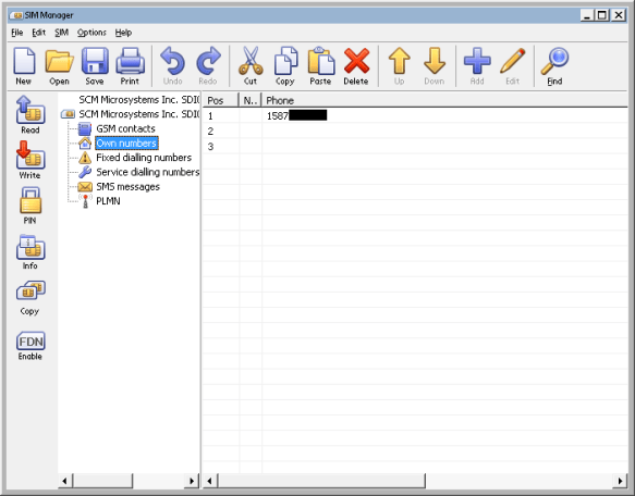
Dekart SIM Manager showing the phone number programmed into the SIM card (censored for privacy).

I tried the PIN in the Dekart SIM Manager software on my computer, and it worked! I was able to read out the contents of the SIM and find out what phone number it used to have, although no other useful information was found.

By using the legacy GSM class 0xA0, I was able to manually verify the PIN by directly communicating with the SIM card using the same command syntax in PC/SC Diagnostic:

SIM Card VERIFY PIN Test

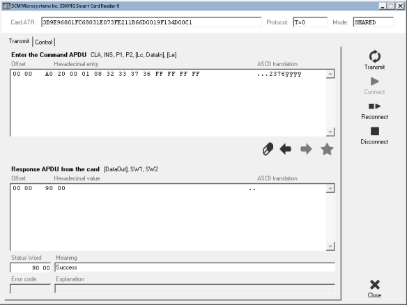
Testing the VERIFY PIN command directly in SpringCard PC/SC Diagnostic.

I took the SIM card out and put it in my Galaxy Core LTE phone, entered the PIN, and as expected it brought up the network unlock prompt. I was able to contact my carrier to get the phone unlocked, and they did it for free (as legally required in Canada) – it turned out to be helpful I was on the same network, as they needed an account to authenticate the request against, even if the phone is registered to another account holder. After entering the 8-digit unlock PIN they provided, the phone was successfully unlocked!

The WF721 is in all likelihood also network locked, but that’s a bridge I haven’t crossed yet.

Conclusion

After a bit of sleuthing into how SIM cards communicate with a cell phone, I was able to decipher the exact command used to authenticate a SIM card PIN inside a disused cellular home phone, all to check if a hand-me-down smartphone was network-locked to its original carrier. Was it a lot of effort just to do that? Maybe, but where’s the fun in buying a prepaid SIM card? 🙂


Advertisement

eMMC Adventures, Episode 4: Recovering data from physically damaged BGA eMMC Flash storage chips

As seen on Hackaday!

The ball grid array (BGA) chip package has been instrumental in getting modern electronics to fit in smaller and smaller spaces, as it uses tiny balls of solder on the bottom of the package to make electrical connections, instead of copper leads on the edge of the chip package. This allows for hundreds of connections to be made in a small amount of PCB area, but their size also makes them very vulnerable to damage as well.

One common way for BGA chips to become damaged is called “pad cratering“, where the copper pad on the package’s substrate (basically a wafer-thin circuit board) separates and leaves behind a crater.

In the case of eMMC (Embedded MultiMediaCard), its package type is known as an FBGA (Fine-pitch Ball Grid Array), so the area of each pad is very small (0.4 mm in diameter!); it doesn’t take much at all to crater the pad – even gently removing solder with solder wick and generous amounts of flux can still cause damage! Most of the pads on an eMMC package are unused, but if any one of the DAT0, CLK, or CMD pads are damaged, then the chip is rendered unusable, even if the chip is placed into a socket for data recovery. If the DAT1-DAT7 pads are damaged, data recovery becomes much slower as the chip is forced to use fewer lines to transmit data (the MMC standard supports data over 1, 4, or 8 lines).

However, there is some hope. Many FBGA packages, including eMMC, use pads that are SMD (solder-mask defined); this means the solder mask is what defines the size of the pad, not the copper itself. Therefore, when the pad gets cratered, often there is a “halo” of copper left behind that still has a chance of getting an electrical connection.

The trick is how to to get a flat conductive area that a chip socket can use to get a reliable connection (without a copper pad, soldering is no longer an option). The eMMC socket adapter I used breaks out the eMMC onto an MMCplus-shaped PCB that can be inserted into any commercial SD card reader.

Filling in the Blanks

There are a few possible materials that can be used to restore contact area on a damaged BGA pad. One possible option is a silver-filled conductive epoxy, but I have not tested its efficacy; an additional consideration is that the volume of the filled-in crater might not be enough to get a filling with sufficiently low resistance for a good connection.

Another option is using solder paste, which I used in this case. Unfortunately, solder’s surface tension is our enemy when trying to fill in a flat area (it wants to form cohesive balls and therefore won’t want to stick to the ring of copper left around the crater), so a means of forcing the solder into the crater requires something flat, rigid and capable of handling the high temperatures experienced during soldering.

At first I tried Kapton (polyimide) tape, but that was a massive failure since it didn’t have the rigidity to stay flat when the solder paste began to melt, and the liquid flux rendered the adhesive useless.

The solution to the issue came in the form of glass. Specifically, I used very thin (0.15 mm thick!) glass “cover slips” normally used to prepare specimens for viewing under a microscope. These can be very inexpensive and one can obtain hundreds of them for a few dollars. The key is to fill the craters with the solder paste by using a knife as a squeegee, then placing the cover slip on top of the eMMC and reflowing it.

It took a few iterations for the pads on some of my eMMC chips to be restored sufficiently, as the volume taken up by the solder will be less than the paste and its accompanying flux. It doesn’t have to fill the entire crater – it just needs to be enough for the eMMC socket’s pins to make a solid connection.

Conclusion

The high-density nature of modern BGA chips is both a blessing and a curse. When trying to do data recovery from devices that use such tiny chips, such as eMMC or UFS Flash storage, sometimes the desoldering process is too much for the chip’s pads to handle. With some ingenuity (and thin glass), it might be possible to temporarily restore enough conductive pad area to get the data off with the help of an eMMC socket.

eMMC Adventures, Episode 3: Building a custom adapter to use cheap eMMC-based 32GB SSD modules

As seen on Hackaday!

While on my quest for more eMMC-based storage devices, I stumbled upon a few devices that piqued my interest: eMMC-based SATA SSDs! I found two models of particular interest: Dell had M.2 modules with a 2.5″ adapter, and HP had custom boards intended for use in cheap laptops (for example, the HP 14-an012nr). Although the former was easier for me to use (but not acquire), I will be focusing on the latter in this blog post.

Overview of HP 14-am/14-an Series SSD Module

Unlike Dell’s convenient M.2 modules, the cheaper boards from HP (costing about $12 USD when I purchased them) had a physical interface intended for use only with its intended host; despite using a SATA interface, physically it used a 10-pin FFC (Flat Flexible Connector, aka “ribbon cable”) since it was designed to work only with HP’s 14-am/14-an series of  low-cost laptops. The boards are labeled “DINERAMD-6050A2862201-DB-A01” and have a copyright date of 2016 in my case.

The BayHub OZ788WR2 Bridge Chip

These eMMC-based SSDs use a curious little chip, the BayHub OZ788WR2 (labeled 788WR2A on the chip itself). It is an SD/MMC-to-SATA adapter, with an SD UHS-II/MMCplus HS200 device interface and SATA II 3Gbps host interface. Apart from the brief description from the manufacturer, no other data is available for the chip (and even finding the chip online is basically impossible).

It’s a shame that so little is known about this chip (and that it’s so rare to find in actual devices), especially since high-performance SD-to-SATA adapters otherwise do not exist, as they use outdated SD-to-CompactFlash adapter chips that are limited to 25 MB/s speeds. If I had the engineering expertise, time, money, and ability to acquire these chips, I’d totally try to make an SD-to-SATA adapter with this chip… but alas, that will still remain a fantasy.

Step 1: Pinout Discovery

The single connector on the eMMC SSD is a ZIF FFC (Zero Insertion Force, Flat Flexible Connector), with no publicly available pinout or any other information. Perhaps this was why I got them for so cheap – apart from holding only 32 GB, nobody could even use them in their own computer even if they wanted to!

When trying to reverse engineer an unknown connector pinout, one needs to first look for ground pins. This is easily accomplished by using a multimeter with a continuity or diode test function, with the multimeter’s positive lead on a known ground point on the DUT (Device Under Test) – screw holes are often good candidates to look for. Ground pins will read as a short, but active IC and power pins will look like a forward-biased diode – appropriately 0.5 to 1 volt. I found 3 power pins (these are often grouped together on connectors for greater current capacity), 3 ground pins, and 4 SATA data pins. The data pins don’t show up on the multimeter test since they have series AC coupling capacitors, but they are easily located next to the connector and have clearly visible differential pairs leading to them.

The issue now is trying to find what order the SATA data pins are in, and how they relate to a regular SATA interface. As it turns out, the pinout is very simple: it matches the pinout of the 7-pin regular SATA interface! This makes sense as the SSD module and the laptop itself are designed to be cheap to manufacture.

Step 2: Building the Adapter (Take 1)

With the pinout known, the harder part is wiring up the connector. However, without a matching connector for the ribbon cable, I have no choice but to solder to it.

As I soon learned, not all flex cables are made of heat-resistant polyimide (aka Kapton) – this one melted before I could even tin the exposed leads. No matter, I’ll just use my trusty magnet wire and hook up the data and power lines! With the help of a salvaged SATA connector from a dead laptop drive, I was able to cobble together a crude adapter for the eMMC SSD board.

Although I didn’t end up taking a picture of the adapter, it wasn’t pretty. It also wasn’t very functional either – although the eMMC SSD board was able to identify itself (on my PC it showed up as a “BHT WR202HH032G E70211F5”), I couldn’t actually perform any data transfer without causing the OZ788WR2 to log hundreds of interface checksum failures (but hey, it supports S.M.A.R.T. data reporting!).

After some tweaking of the wire spacing, I was able to get the adapter stable enough to work, and encased it in hot glue for protection. It lasted a few weeks but eventually stopped working because one of the data wires broke off inside the blob of hot glue. Additionally, the outer contacts on the ribbon cable connector were peeling away from its plastic substrate. It was time for a rebuild.

Step 3: Building a Dedicated eMMC SSD (the teaser!)

Since I had multiple eMMC SSD boards, I took one, replaced the eMMC with a 128GB one from Samsung (the KLMDG8JENB-B041) and removed the ribbon cable connector. In its place, I used some very thin twinaxial cable from a dead MacBook and used a gutted CFast-to-SATA adapter for a shell. Stay tuned for that in another blog post!

Step 4: Building the Adapter (again!)

Much like my previous attempt, I used a salvaged PCB from a dead laptop drive, but left a lot of it instead of chopping it off directly at the connector. This particular one was a dead Samsung HDD, and it had one particular feature that I could use to make a stronger adapter: it had a TSOP footprint for the DRAM cache, which was just the right pitch for me to solder the ribbon cable to!

With a little help of my hot air rework station, I removed the DRAM cache and DC-DC converter, leaving the SATA AC coupling capacitors and the power input components (filtering choke and capacitors, and input overvoltage protection) behind.

After scraping off some solder mask, I soldered the SATA data wires and the ground wires surrounding them with very thin magnet wire, trying to keep the data pairs as close to each other as possible to minimize the chance of interference causing problems. The power wire was soldered to the power input components, right next to the input capacitor for better power delivery.

After checking with the multimeter that no short circuits were present, I hooked up an eMMC board and plugged it into my PC. It enumerated without issues, and running several tests including CrystalDiskMark, h2testw, and Hard Disk Sentinel’s random read test, amassing several hundreds of gigabytes in reads and writes with zero CRC errors logged in the S.M.A.R.T. data.

With everything checked out, I cleaned the circuit with isopropyl alcohol and covered the exposed end of the ribbon cable and the magnet wires with clear epoxy for protection. I also used a bit of epoxy on the flex connector to re-secure the lifted contacts to the substrate.

Conclusion

With a bit of wire and a circuit board from a dead HDD, I was able to reuse cheap eMMC-based SATA SSDs on computers that they weren’t meant for (and they even had copies of Windows 10 Home with extractable license keys! 🙂 ). Although not as fast as a modern full-fledged SSD, its relatively high 4K IOPS performance means it works well enough as a quick boot drive for running quick tests of OS installation without needing to sacrifice a bigger drive just for testing – and they consume less than a watt even when fully active!

Tutorial: Recovering Cookie Clicker saves from an offline installation/backup of Google Chrome

Update (August 29, 2018): Turns out cleaning out your cookies/cache will erase your Cookie Clicker save. Who would’ve thought…

Cookie Clicker saves: You don’t realize the importance of saving your progress until you lose your save data. A few days ago I opened Chrome to my always-running instances of Cookie Clicker, but found that all of my progress was deleted (and it was showing a “Don’t forget to back up your save” message just to add insult to injury).

My heart sank when I realized that one of my runs, over three years old, had suddenly vanished into thin air. I tried restoring Google Chrome’s data via a Shadow Copy; no dice. I tried using my Windows Home Server 2011 backups, but realized that it would take over an hour to restore my Chrome folder. After much frustration, I decided to retrieve and examine Chrome’s Local Storage folder and see whether I could retrieve my save files that way – and it worked! Here’s how to recover your own Cookie Clicker saves…

Retrieving an older version of Google Chrome’s data folder

If you have Shadow Copy (aka Previous Versions) enabled, you may be in luck if the restore point(s) available have intact game save information. If you have an offline backup solution, that may be usable as well. If you have neither, you could try it on your current Chrome installation but your chances of recovery are much slimmer.

For Windows, Google Chrome’s default Local Storage folder located at: %USERPROFILE%\AppData\Local\Google\Chrome\User Data\Default\Local Storage

There will probably be a large number of files ending in .localstorage and .localstorage-journal – these are unlikely to contain your saves, and if they are present, they will be many months out of date; Google has begun storing websites’ local storage in a LevelDB database. The database in question is stored in a folder called leveldb.

If you are attempting to retrieve the data from a current Chrome installation, close Chrome before continuing.

Copy this “leveldb” folder to another (safe) location as to avoid any accidental overwrite of the database while trying to recover the game saves. Download and install the FastoNoSQL database browser software (it’s a trial, but for our purposes it will do just fine – just follow the registration instructions and you can whip up a temporary email address if you need to).

Browsing the LevelDB database

When FastoNoSQL is opened for the first time, the Connections window will appear. Click the “Add connection” button (it looks like a green button with a + symbol on it); even though we’re just browsing some database files, it’s considered to be a “connection” to the database. Select “LevelDB” and choose the folder that holds the “leveldb” folder that was previously copied.

Once the database is opened, note the number of database keys (in my case it was 1212), right-click the “default” database in the Explorer tree on the left-hand side of the FastoNoSQL window, and select “Load content of database”. Enter the number of keys previously noted into the “Keys count” field, then click OK.

In the “Search…” box, enter this text (select all the text in this box):

\\x5f\\x68\\x74\\x74\\x70\\x73\\x3a\\x2f\\x2f\\x6f\\x72\\x74\\x65\\x69\\x6c\\x2e\\x64\\x61\\x73\\x68\\x6e\\x65\\x74\\x2e\\x6f\\x72\\x67\\x00\\x01\\x43\\x6f\\x6f\\x6b\\x69\\x65\\x43\\x6c\\x69\\x63\\x6b\\x65\\x72\\x47\\x61\\x6d\\x65

This cryptic-looking text is a hexadecimal-escaped version of the string _https://orteil.dashnet.org, an SOH (Start of Header) character, and CookieClickerGame.

If your saves are found, you will see one or two entries, depending on whether or not the normal and/or Beta saves are present. The first entry will be the normal version of Cookie Clicker, and the second one, with a slightly longer key (ending in “\x42\x65\x74\x61”) is the for the Beta. Right-click the desired entry and choose “Edit…” to view the game save data. Copy the contents of the “Value” field into a text editor (Notepad, etc.), and delete the very first character before “Mi4w” – this is an SOH (Start of Header) character and we don’t need it to restore the game save. Save this text file so you have a backup of your game save, and import the file into Cookie Clicker (either by copy-pasting the text or using the “Load from file” button).

The game save should look like this (look for the bolded characters to ensure the game save data is intact):
Mi4wMDQ1fHwxNTI [... text omitted ...] OkwoDCgAR8%21END%21

If everything works out, your Cookie Clicker game save should be restored from the brink of destruction!