Unboxing and review of SanDisk 64GB microSDXC High Endurance Card

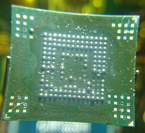
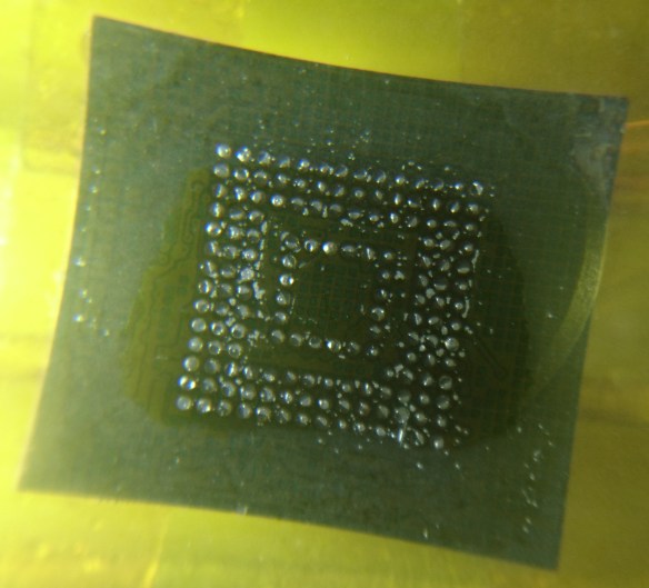
UPDATE (July 19, 2020): I’ve analyzed a 128GB version of the High Endurance card, and it appears that SanDisk is using 3D TLC Flash.

Dashcams: they can be a crucial tool when reconstructing events in a vehicular incident, or a source of entertainment when watching compilations on YouTube. Like any modern device, they generally use SD or microSD cards as their storage medium. However, not all cards are created equal.

Cheaper cards, like SanDisk’s Ultra lineup, use cheaper TLC (triple-level cell) NAND Flash that is ill-suited to the harsh working conditions of a dashcam. Not only does the card have to endure temperature extremes, the constant writes can burn through the Flash’s write cycles in short order. In fact, SanDisk specifically denounces this line of cards for use in continuous-recording applications.

The solution: high-endurance memory cards! These cards (at least in theory) use more durable MLC or even SLC NAND Flash, which can take many more write cycles. I purchased the 64-gigabyte model, the SDSQQNR-064G-G46A.

Unboxing

The card’s packaging isn’t much different than SanDisk’s typical microSD card offerings. The paper-and-plastic package includes a small blister pack that holds the microSD card itself and the full-size SD card adapter, without a carrying case (granted, the memory card is expected to stay inside the dashcam for most of its working life).

The packaging also includes a license key for a 1-year subscription to the RescuePRO data recovery software (although in all honesty, you’d be better off using the free PhotoRec software instead).

Endurance Rating

SanDisk’s lineup of high-endurance memory cards are designed for use in very write-intensive workloads, such as constant video recording.

Unfortunately, the endurance specifications for these cards are (probably intentionally) vague, only providing a set number of hours of video recording. However, we can infer a rating with a little bit of math.

SanDisk’s card packaging defines Full HD video to be 26 Mbps, which is equivalent to 3.25 (binary) megabytes per second. This equates to 11,700 megabytes per hour, or 11.426 gigabytes per hour. With a rating of 5,000 hours at this data rate, we get a specified endurance of 57,128.91 gigabytes written, or 55.79 terabytes written (TBW).

Memory cards, like other block-based storage media, often define capacities with decimal prefixes, whereas computers usually binary. A “64-gigabyte” card is really 59.605 binary gigabytes (“gibibytes“) in capacity, but in this blog post I’m using the Windows notation of gigabytes; that is, calculating in binary but displaying as decimal. 😛

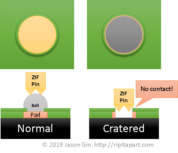
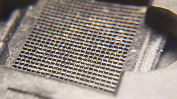
Therefore, we get a final calculated P/E (program-erase) cycle count of… 936 cycles. This is more in line with traditional 2D TLC NAND Flash, so I suspect that this rating is either based on different bitrates, or SanDisk is being really, really conservative in their estimates – or heck, maybe this really is just TLC NAND Flash that’s being configured and/or warrantied differently by SanDisk. As much as I am tempted to remove the epoxy coating that covers the manufacturing test pads in order to get a NAND Flash signature directly, I like having a warranty for at least a few years. Maybe I’ll buy another card to try this on…

UPDATE (July 19, 2020): I got my paws on another card (the 128GB variant), and did some reverse-engineering work on it to determine what Flash SanDisk used. It turns out they used 3D TLC NAND, which is still quite durable and reliable due to the use of larger process geometries. The Flash should easily withstand thousands of write cycles without much issue.

Card Information

Using an older laptop with a true SD-compliant slot (most newer ones are just USB card readers internally), I was able to grab the card’s metadata from Linux. These information files are found in /sys/block/mmcblkX/device, where X is usually 0 depending on your host machine. Android used to be able to do this as well, but nowadays it’s not possible without a rooted operating system.

Item Value
CID (Card ID) 035744534836344780ed1bbb9e013100
CSD (Card Specific Data) 400e0032db790001dbd37f800a404000
Manufacturer ID 0x03 (SanDisk)
Manufacture Date January 2019
Device Name SH64G
Firmware Version 0x0
Hardware Revision 0x8

Initial Formatting

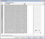
The card is formatted as exFAT, with a 16 MB offset (that is, the first 16 MB of the card is unallocated), with an allocation unit size of 128 kilobytes. It uses a very basic MBR (Master Boot Record) partition structure, with the first sector being the bare minimum to be recognized as a valid structure.
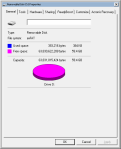
Performance

Now that I’ve probably irked some of my readers with my usage of decimal and binary prefixes, it’s time to see how fast this card can go. SanDisk’s own ratings for the card are very brief, citing a sequential read/write speed of 100 and 40 MB/s respectively. It is rated for the V30 Video speed classification, which guarantees a minimum of 30 MB/s sequential writes continuously.

All the tests below were performed on my desktop computer using a FCR-HS4 USB 3.0 reader from Kingston, which is based on the Realtek RTS5321 chipset.

CrystalDiskMark

CrystalDiskMark is the de-facto standard for storage benchmarks. I’m using the 64-bit edition of CDM, version 5.2.0.

I/O Type Read Write
Sequential QD32 91.80 MB/s 60.56 MB/s
Sequential 93.33 MB/s 61.66 MB/s
4K Random QD32 8.319 MB/s
2129.7 IOPS
4.004 MB/s
1025.0 IOPS
4K Random 8.121 MB/s
2079.0 IOPS
3.971 MB/s
1016.6 IOPS

The sequential I/O speeds are on par with a modern microSDXC card, and the IOPS aren’t too shabby either; they exceed the IOPS requirements for the A1 performance class which requires R/W IOPS of 1500 and 500 respectively. This could make this type of card a viable option for other write-heavy environments – this includes single-board computers (SBCs) like the Raspberry Pi, where memory card failures due to excessive writes are common.

ATTO Disk Benchmark

The card’s read/write performance levels off at around the 64-kilobyte mark during testing, showing that operations smaller than this incur a significant performance penalty. This may also be indicative of the internal page and block sizes of the NAND Flash itself.

Hard Disk Sentinel

Hard Disk Sentinel comes with a bunch of disk benchmarking tools, including some to test the entire “surface” of a drive. I used the software’s Surface Test tool to measure the card’s performance before and after filling the drive with data – first with random data, then with all zeroes.

Random Seek Test

The Random Seek Test measures the card’s latency when performing random “seeks”, although more accurately it reads a single sector from a random location.

State Average Latency Minimum Latency Maximum Latency
Empty/Initial (0x00) 360 µs 350 µs 420 µs
Random Fill 600 µs 590 µs 670 µs
Zero Fill 600 µs 590 µs 690 µs

The card initially had about 420 microseconds of latency, but after filling the card with random data, this increased to 670 microseconds. Filling the card with all zeroes again did not improve performance, and his isn’t helped by the fact that SD cards generally lack the ability to “TRIM” unused sectors like SSDs or eMMC chips.

Full Surface Read (or at least an attempt)
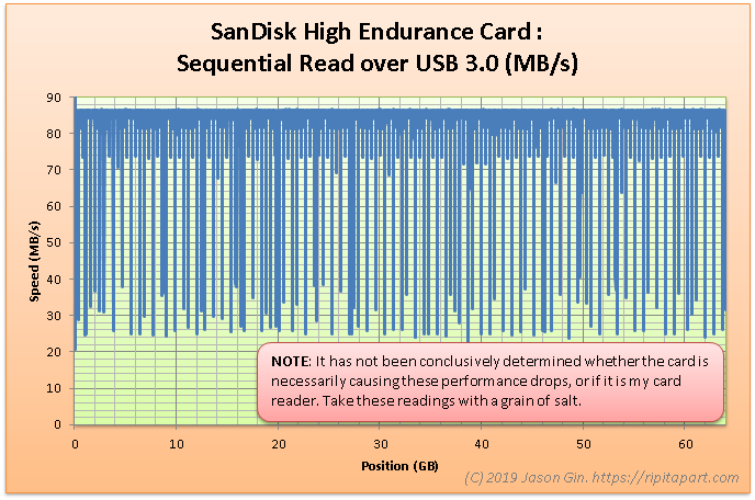
This is where things get a bit… interesting. It was around this time that I noticed some performance inconsistencies that didn’t show up on other benchmarks. Although the I/O speeds largely matched what my other benchmarks revealed, I noticed frequent dips below normal, often down to the mid-20 MB/s range! I wasn’t sure that this was necessarily the card’s fault (pauses in read/writes could result in performance degradation on a device if it can’t buffer the writes well enough), or if my card reader/operating system/etc. was responsible.

I decided to hold off on publishing the sequential write test until I get this issue figured out – perhaps it’s worthy of a blog post all on its own…

Advertisement

eMMC Adventures, Episode 4: Recovering data from physically damaged BGA eMMC Flash storage chips

As seen on Hackaday!

The ball grid array (BGA) chip package has been instrumental in getting modern electronics to fit in smaller and smaller spaces, as it uses tiny balls of solder on the bottom of the package to make electrical connections, instead of copper leads on the edge of the chip package. This allows for hundreds of connections to be made in a small amount of PCB area, but their size also makes them very vulnerable to damage as well.

One common way for BGA chips to become damaged is called “pad cratering“, where the copper pad on the package’s substrate (basically a wafer-thin circuit board) separates and leaves behind a crater.

In the case of eMMC (Embedded MultiMediaCard), its package type is known as an FBGA (Fine-pitch Ball Grid Array), so the area of each pad is very small (0.4 mm in diameter!); it doesn’t take much at all to crater the pad – even gently removing solder with solder wick and generous amounts of flux can still cause damage! Most of the pads on an eMMC package are unused, but if any one of the DAT0, CLK, or CMD pads are damaged, then the chip is rendered unusable, even if the chip is placed into a socket for data recovery. If the DAT1-DAT7 pads are damaged, data recovery becomes much slower as the chip is forced to use fewer lines to transmit data (the MMC standard supports data over 1, 4, or 8 lines).

However, there is some hope. Many FBGA packages, including eMMC, use pads that are SMD (solder-mask defined); this means the solder mask is what defines the size of the pad, not the copper itself. Therefore, when the pad gets cratered, often there is a “halo” of copper left behind that still has a chance of getting an electrical connection.

The trick is how to to get a flat conductive area that a chip socket can use to get a reliable connection (without a copper pad, soldering is no longer an option). The eMMC socket adapter I used breaks out the eMMC onto an MMCplus-shaped PCB that can be inserted into any commercial SD card reader.

Filling in the Blanks

There are a few possible materials that can be used to restore contact area on a damaged BGA pad. One possible option is a silver-filled conductive epoxy, but I have not tested its efficacy; an additional consideration is that the volume of the filled-in crater might not be enough to get a filling with sufficiently low resistance for a good connection.

Another option is using solder paste, which I used in this case. Unfortunately, solder’s surface tension is our enemy when trying to fill in a flat area (it wants to form cohesive balls and therefore won’t want to stick to the ring of copper left around the crater), so a means of forcing the solder into the crater requires something flat, rigid and capable of handling the high temperatures experienced during soldering.

At first I tried Kapton (polyimide) tape, but that was a massive failure since it didn’t have the rigidity to stay flat when the solder paste began to melt, and the liquid flux rendered the adhesive useless.

The solution to the issue came in the form of glass. Specifically, I used very thin (0.15 mm thick!) glass “cover slips” normally used to prepare specimens for viewing under a microscope. These can be very inexpensive and one can obtain hundreds of them for a few dollars. The key is to fill the craters with the solder paste by using a knife as a squeegee, then placing the cover slip on top of the eMMC and reflowing it.

It took a few iterations for the pads on some of my eMMC chips to be restored sufficiently, as the volume taken up by the solder will be less than the paste and its accompanying flux. It doesn’t have to fill the entire crater – it just needs to be enough for the eMMC socket’s pins to make a solid connection.

Conclusion

The high-density nature of modern BGA chips is both a blessing and a curse. When trying to do data recovery from devices that use such tiny chips, such as eMMC or UFS Flash storage, sometimes the desoldering process is too much for the chip’s pads to handle. With some ingenuity (and thin glass), it might be possible to temporarily restore enough conductive pad area to get the data off with the help of an eMMC socket.

eMMC Adventures, Episode 3: Building a custom adapter to use cheap eMMC-based 32GB SSD modules

As seen on Hackaday!

While on my quest for more eMMC-based storage devices, I stumbled upon a few devices that piqued my interest: eMMC-based SATA SSDs! I found two models of particular interest: Dell had M.2 modules with a 2.5″ adapter, and HP had custom boards intended for use in cheap laptops (for example, the HP 14-an012nr). Although the former was easier for me to use (but not acquire), I will be focusing on the latter in this blog post.

Overview of HP 14-am/14-an Series SSD Module

Unlike Dell’s convenient M.2 modules, the cheaper boards from HP (costing about $12 USD when I purchased them) had a physical interface intended for use only with its intended host; despite using a SATA interface, physically it used a 10-pin FFC (Flat Flexible Connector, aka “ribbon cable”) since it was designed to work only with HP’s 14-am/14-an series of  low-cost laptops. The boards are labeled “DINERAMD-6050A2862201-DB-A01” and have a copyright date of 2016 in my case.

The BayHub OZ788WR2 Bridge Chip

These eMMC-based SSDs use a curious little chip, the BayHub OZ788WR2 (labeled 788WR2A on the chip itself). It is an SD/MMC-to-SATA adapter, with an SD UHS-II/MMCplus HS200 device interface and SATA II 3Gbps host interface. Apart from the brief description from the manufacturer, no other data is available for the chip (and even finding the chip online is basically impossible).

It’s a shame that so little is known about this chip (and that it’s so rare to find in actual devices), especially since high-performance SD-to-SATA adapters otherwise do not exist, as they use outdated SD-to-CompactFlash adapter chips that are limited to 25 MB/s speeds. If I had the engineering expertise, time, money, and ability to acquire these chips, I’d totally try to make an SD-to-SATA adapter with this chip… but alas, that will still remain a fantasy.

Step 1: Pinout Discovery

The single connector on the eMMC SSD is a ZIF FFC (Zero Insertion Force, Flat Flexible Connector), with no publicly available pinout or any other information. Perhaps this was why I got them for so cheap – apart from holding only 32 GB, nobody could even use them in their own computer even if they wanted to!

When trying to reverse engineer an unknown connector pinout, one needs to first look for ground pins. This is easily accomplished by using a multimeter with a continuity or diode test function, with the multimeter’s positive lead on a known ground point on the DUT (Device Under Test) – screw holes are often good candidates to look for. Ground pins will read as a short, but active IC and power pins will look like a forward-biased diode – appropriately 0.5 to 1 volt. I found 3 power pins (these are often grouped together on connectors for greater current capacity), 3 ground pins, and 4 SATA data pins. The data pins don’t show up on the multimeter test since they have series AC coupling capacitors, but they are easily located next to the connector and have clearly visible differential pairs leading to them.

The issue now is trying to find what order the SATA data pins are in, and how they relate to a regular SATA interface. As it turns out, the pinout is very simple: it matches the pinout of the 7-pin regular SATA interface! This makes sense as the SSD module and the laptop itself are designed to be cheap to manufacture.

Step 2: Building the Adapter (Take 1)

With the pinout known, the harder part is wiring up the connector. However, without a matching connector for the ribbon cable, I have no choice but to solder to it.

As I soon learned, not all flex cables are made of heat-resistant polyimide (aka Kapton) – this one melted before I could even tin the exposed leads. No matter, I’ll just use my trusty magnet wire and hook up the data and power lines! With the help of a salvaged SATA connector from a dead laptop drive, I was able to cobble together a crude adapter for the eMMC SSD board.

Although I didn’t end up taking a picture of the adapter, it wasn’t pretty. It also wasn’t very functional either – although the eMMC SSD board was able to identify itself (on my PC it showed up as a “BHT WR202HH032G E70211F5”), I couldn’t actually perform any data transfer without causing the OZ788WR2 to log hundreds of interface checksum failures (but hey, it supports S.M.A.R.T. data reporting!).

After some tweaking of the wire spacing, I was able to get the adapter stable enough to work, and encased it in hot glue for protection. It lasted a few weeks but eventually stopped working because one of the data wires broke off inside the blob of hot glue. Additionally, the outer contacts on the ribbon cable connector were peeling away from its plastic substrate. It was time for a rebuild.

Step 3: Building a Dedicated eMMC SSD (the teaser!)

Since I had multiple eMMC SSD boards, I took one, replaced the eMMC with a 128GB one from Samsung (the KLMDG8JENB-B041) and removed the ribbon cable connector. In its place, I used some very thin twinaxial cable from a dead MacBook and used a gutted CFast-to-SATA adapter for a shell. Stay tuned for that in another blog post!

Step 4: Building the Adapter (again!)

Much like my previous attempt, I used a salvaged PCB from a dead laptop drive, but left a lot of it instead of chopping it off directly at the connector. This particular one was a dead Samsung HDD, and it had one particular feature that I could use to make a stronger adapter: it had a TSOP footprint for the DRAM cache, which was just the right pitch for me to solder the ribbon cable to!

With a little help of my hot air rework station, I removed the DRAM cache and DC-DC converter, leaving the SATA AC coupling capacitors and the power input components (filtering choke and capacitors, and input overvoltage protection) behind.

After scraping off some solder mask, I soldered the SATA data wires and the ground wires surrounding them with very thin magnet wire, trying to keep the data pairs as close to each other as possible to minimize the chance of interference causing problems. The power wire was soldered to the power input components, right next to the input capacitor for better power delivery.

After checking with the multimeter that no short circuits were present, I hooked up an eMMC board and plugged it into my PC. It enumerated without issues, and running several tests including CrystalDiskMark, h2testw, and Hard Disk Sentinel’s random read test, amassing several hundreds of gigabytes in reads and writes with zero CRC errors logged in the S.M.A.R.T. data.

With everything checked out, I cleaned the circuit with isopropyl alcohol and covered the exposed end of the ribbon cable and the magnet wires with clear epoxy for protection. I also used a bit of epoxy on the flex connector to re-secure the lifted contacts to the substrate.

Conclusion

With a bit of wire and a circuit board from a dead HDD, I was able to reuse cheap eMMC-based SATA SSDs on computers that they weren’t meant for (and they even had copies of Windows 10 Home with extractable license keys! 🙂 ). Although not as fast as a modern full-fledged SSD, its relatively high 4K IOPS performance means it works well enough as a quick boot drive for running quick tests of OS installation without needing to sacrifice a bigger drive just for testing – and they consume less than a watt even when fully active!