As seen on Hackaday!
TL;DR: Disposable vapes can have LCD screens…?! At least they’re moddable now – check out my GitHub for docs, tools, and links to similar projects if you want to try this on a Kraze HD7K or Raz TN9000 (maybe some others too).
Disposable vaping devices have become distressingly common in recent years, and an increasing ecological burden given how many (perfectly reusable!) lithium-ion batteries are discarded into landfills and roadsides alike. Even worse, some of them include flashy colour LCD screens! I’ve been collecting and harvesting disposable vapes from my friends for a few years now, but only recently have I had a chance to take some of these LCD-equipped models apart; while doing so, I figured I could pioneer some reverse-engineering efforts while adding custom theme/skin support along the way. (For the record, I don’t vape or smoke but plenty of my friends do. I’m just in it for the batteries and electronics.)

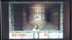
A modified Kraze HD7K disposable vape, with my custom Windows 95 theme applied.
The vape in question is found in my area of Canada as the Kraze HD7K, but it seems to go by other names like the Raz TN9000. Internally, they are the same minus some firmware and logo differences.
Disclaimer & Safety Information
Harvesting disposable vapes is not without its own risks, and I will not accept any responsibility if something goes wrong if you try it yourself. This should only be attempted if you are familiar with handling lithium-ion batteries and the safety implications that they pose.
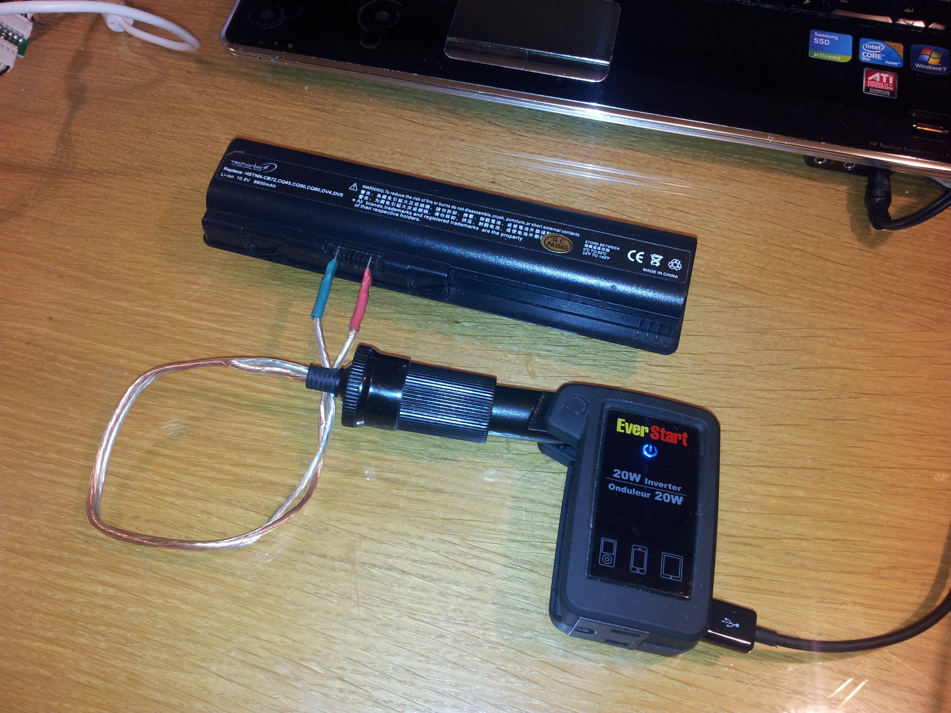
Nicotine can enter your bloodstream simply by getting vape juice on your skin (so wear gloves!), and can be messy if it gets on your clothes and workspace. The enclosed lithium-ion battery can also cause burns or property damage if short-circuited, and are usually not equipped with protection circuits; the fact that these cells can push several amps in such a small package is the precise reason they’re (wastefully) used in this application. Rechargeable disposable vapes pose a slightly higher risk if the cell is near or at full charge when disassembled, whereas pure disposables are almost always fully discharged. Discharged cells inherently hold less energy and this reduces the fire risk should a catastrophic failure occur during disassembly, but they still need to be treated with respect. Overdischarged cells below 2 volts may not necessarily recover, but if you decide to attempt a recovery, you must bring them back up to 3 volts at a very low current (on the order of tens of milliamps), after which it is possible to charge them normally.
Vapes harvested from the roadside should only be picked up when it is safe to do so, and should be inspected for damage as soon as possible. These “street lithium” vapes could be water-damaged and also physically damaged from getting run over by vehicles. Any cells with a punctured or torn pouch/casing are unsalvageable and must be recycled. My own experimental data finds that the majority of run-over cells survive, but I would not recommend using them without being absolutely sure that there is no further internal damage (after charging the cell with supervision, it should have at least 90% of its rated capacity and no appreciable self-discharge after a few weeks of rest. Otherwise, put it in the recycle bin where it belongs). Even then, only use them in applications where their failure will not cause collateral damage, like in an outdoor solar-powered lamp that is kept away from anything flammable. If you’re not comfortable with these conditions, just recycle the vape at an appropriate facility in accordance with local regulations (some vape shops will have recycling bins, and hardware stores often will accept rechargeable batteries for recycling too).
Teardown
Without any screw holes, I needed to find another way to (non-destructively) open the vape. I noticed a seam in the bottom end cap, and found that sliding a slotted screwdriver into that seam and some gentle prying action was able to dislodge the internal clips. Once that cap was free, a sliding airflow “switch” fell out as well. Removing the core of the vape was pretty straightforward, but it did require some pliers to pull it out due to its friction-fit construction.
-

- Removed end cap. The airflow restriction switch falls out easily.
-

- The core of the Kraze vape slides out with pliers.
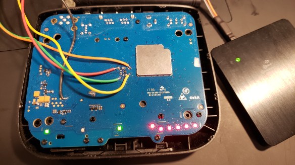
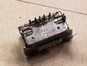
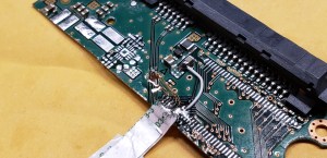
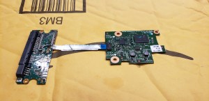
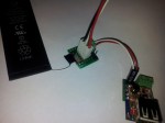
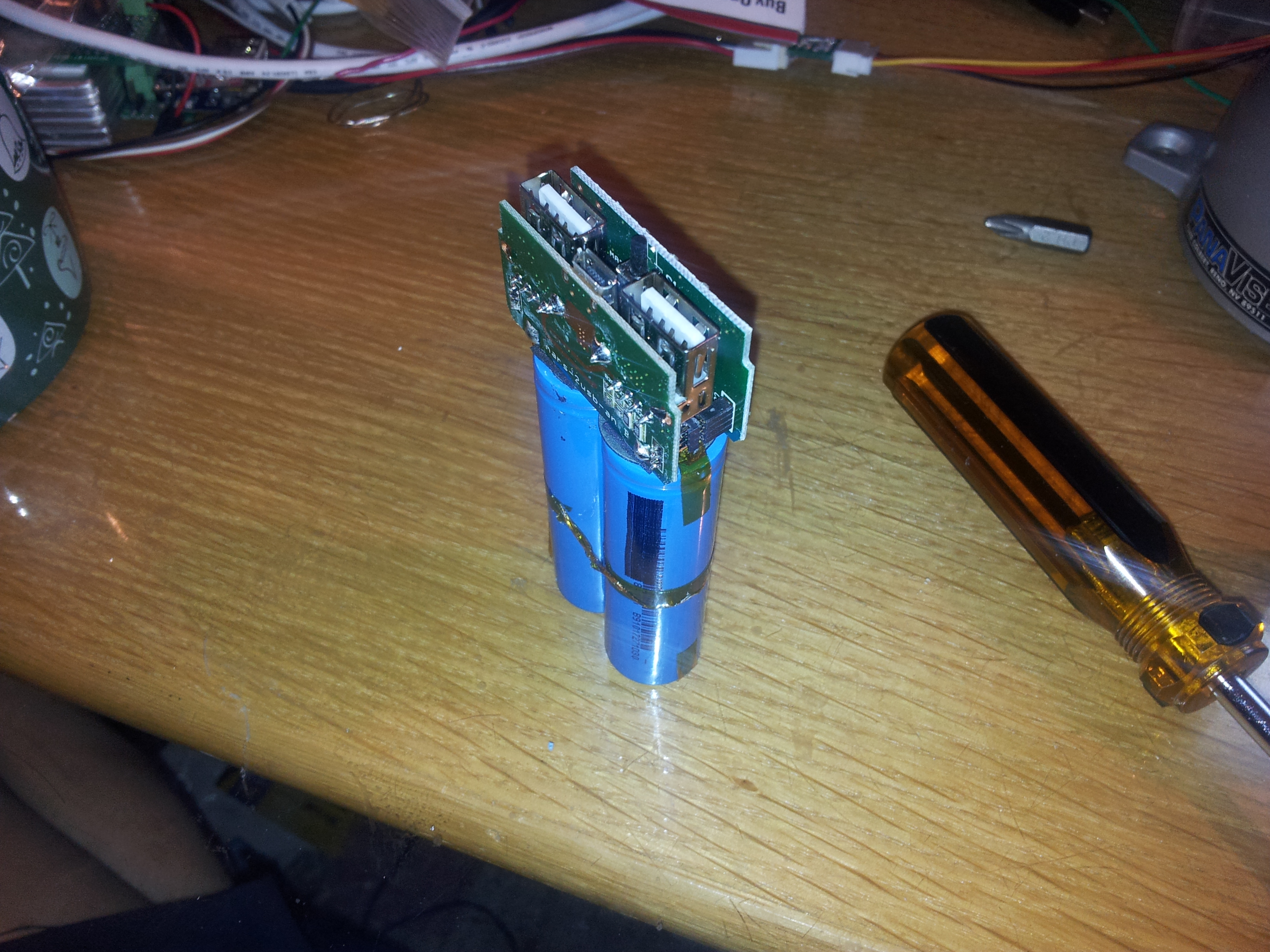
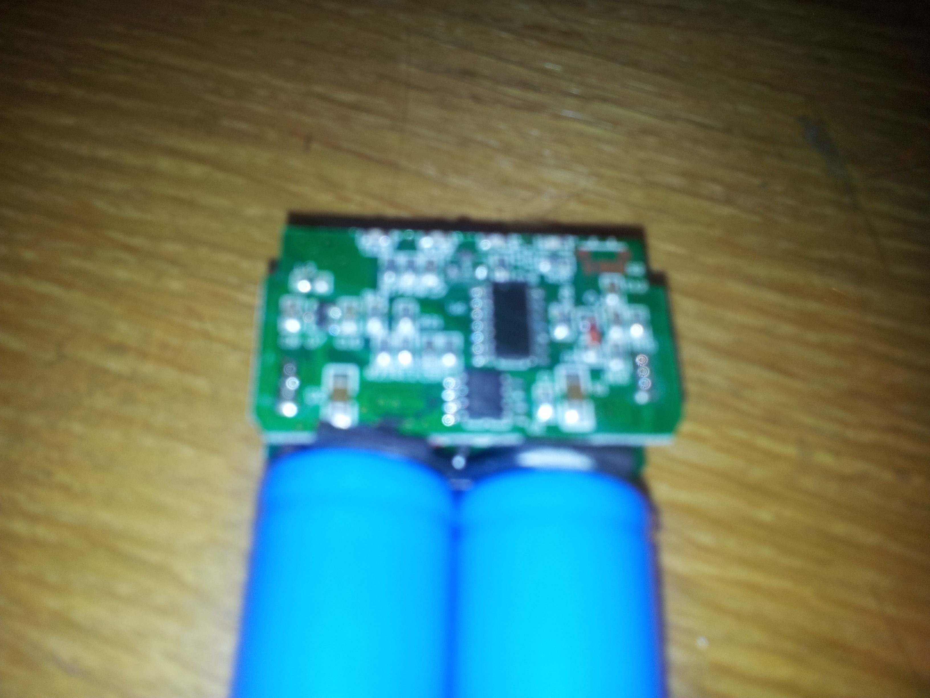
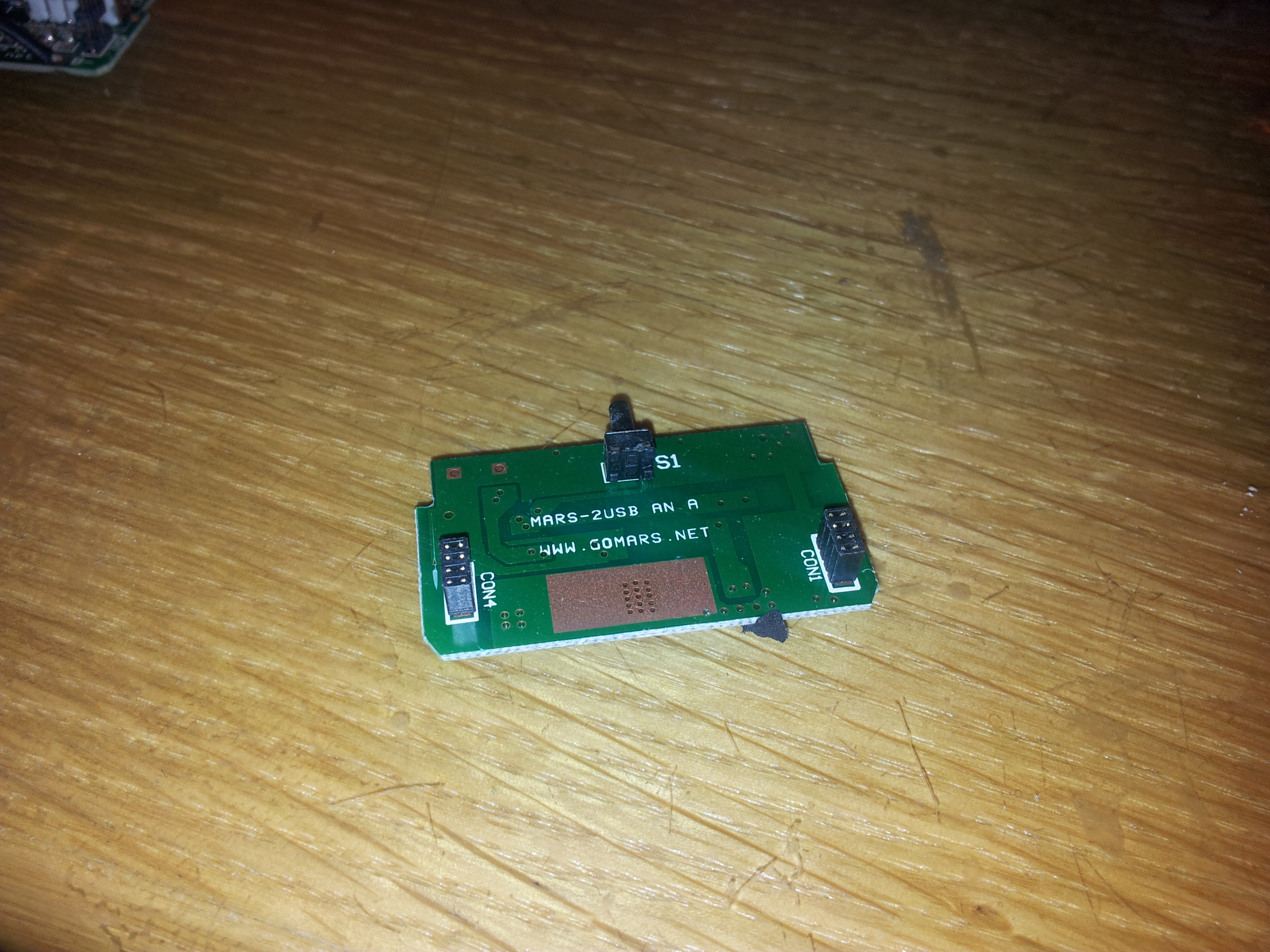
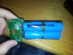
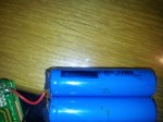
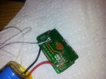
With the core exposed, I could see that the vape uses a 13450-size lithium-ion pouch cell (13mm diameter, 45mm length) and a generously-sized vape juice reservoir, with a sponge to absorb the juice and prevent it from leaking. I also noticed a small 9-pin right angle header that connected a black “logic board” that held a microcontroller and LCD screen, and a green “power board” that had the inhalation sensor, heating coil connector, USB-C connector and solder pads for the battery.
-

- Exposed core with 13450-size battery and large juice reservoir.
-

- The Kraze’s internals while power is applied through USB-C.
Reverse-Engineering
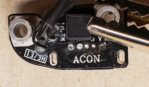
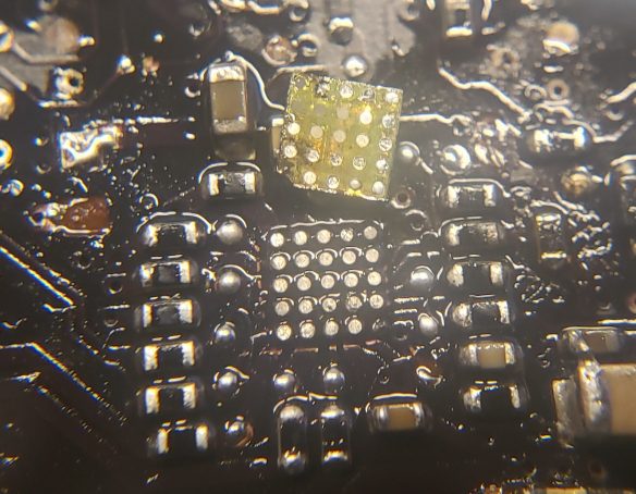
The three main components of the vape’s logic board are the microcontroller, an SPI NOR Flash chip, and the LCD screen.
-

- Nations Tech N32G031K8Q7-1 microcontroller and Giantech GT25Q80A-UZLI SPI Flash.
-

- LCD ribbon cable, part number FXD096QQ08B-F.
The microcontroller is a Nations Tech N32G031K8Q7-1, containing a 48MHz Arm Cortex-M0 CPU, 64k of internal Flash and 8k of SRAM; the SPI Flash is a 1MB Giantech GT25Q80A-UZLI; and the LCD is of an unknown maker but has a part number of FXD096QQ08B-F, with a resolution of 80×160 pixels.
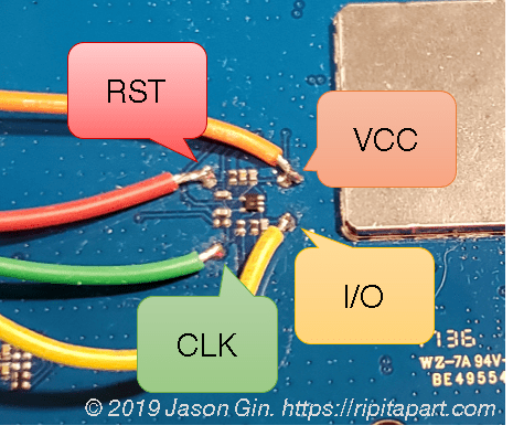
Given that the LCD is what makes this vape particularly special, I decided to look into what controller and pinout it uses. I had a hunch that it would use a common interface and controller (to keep costs low), and searched for a 0.96″ LCD with 13-pin FPC (flexible printed circuit) connector. This led me to the Smart Prototyping #102106, which used a 13-pin connector and seemed to have a compatible pinout. The aforementioned LCD uses a common ST7735S controller, and is controlled through a 4-wire SPI interface (clock, data, command/data select, chip select). (Additionally, I looked on Alibaba for a similar LCD, and found one source that sells them for about $1.25 each in large quantities; this suggests that the displays themselves add significant cost to the vape, but are still cheap enough to be utilized in a throwaway device.)
I searched other websites for LCDs with the same dimensions and connector, and they all used this pinout:
| Pin | Name | Function |
|---|---|---|
| 1 | TP0/NC | Unused (may be used for some touch sensor?) |
| 2 | TP1/NC | Unused (may be used for some touch sensor?) |
| 3 | SDIN | SPI data to LCD |
| 4 | SCLK | SPI clock |
| 5 | RS | Logic low = command, high = data |
| 6 | /RST | Reset (active-low) |
| 7 | /CS | Chip select (active-low) |
| 8 | GND | Power supply/signal ground |
| 9 | NC | Not connected |
| 10 | VDD | Power supply (3.3V) |
| 11 | LEDK | LED backlight cathode |
| 12 | LEDA | LED backlight anode |
| 13 | GND | Power supply/signal ground |
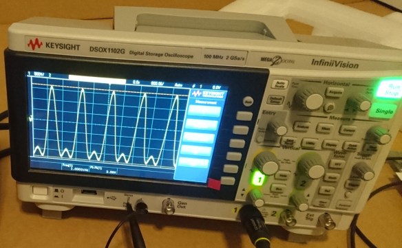
To ensure that the pinout I was looking at really matched up with what was in the vape, I connected the data, clock and other control lines to my DSLogic Plus logic analyzer and sniffed the traffic as the vape initializes the display. A glance at the logic analyzer data confirmed the pinout.
-

- Wires connected to LCD for traffic sniffing.
-

- Screenshot of DSView reading the LCD SPI data.
To further confirm that I had an ST7735S-based display, I resoldered the LCD onto a TSSOP-to-DIP breakout board (which was annoying, as the pin pitch was slightly different and alignment needed much precision), and used the Adafruit Graphics Library and ST7735S driver on a Teensy 3.0 microcontroller, and it worked! Well, mostly. While black-and-white text worked perfectly, the red and blue channels seem to be swapped around when using the tft.initR(INITR_MINI160x80) routine, and it seems that I wasn’t the only one with this issue.
-

- The classic “lorem ipsum” sample text on the LCD from the Kraze HD7K vape.
-

- Notice how the red and blue text seem to be swapped.
I decided I was finished with the idea of reusing the display alone, and began looking into how the vape itself works, and how it displays images. The first step was to look into the memory contents of the 1MB SPI Flash, as that is a pretty large amount of memory for such a simple device. I desoldered the chip and mounted it on a SSOP-to-DIP adapter, and dumped its contents to a file using my MiniPro TL866CS universal programmer.
-

- Data streamed from the SPI Flash to the LCD.
-

- LCD data stored in the SPI Flash.
-

- A closeup of the top-left of the main screen. Notice the blue pixels coinciding with the raw data.
My suspicions were confirmed when I analyzed the image data being sent to the LCD matching what was in the beginning of the SPI Flash. The data also looked like it was in a raw “RGB565” format, which is a method of packing a 16-bit pixel into two bytes of data; the term “565” refers to 5, 6, and 5 bit values belonging to the red, blue and green channels respectively. Since the image on the screen used blue in the top-left of the image, this supported my findings since the data similarly had only set bits belonging to the blue channel, and also further describes the data as being “big-endian” assuming that the red bits are read out before the green and blue.
The data seemed to be transferred in 4096-byte blocks, which I speculated to be performed using DMA (direct memory access); the data transfers seemed too fast and regular to be done in software alone. This later proved to be true when I had a chance to analyze the RAM of a working vape.
(Flash) Map-Making
With the 1MB SPI Flash chip dumped, it was time to take that apart too… but digitally! Armed with a spreadsheet, a hex editor, ImageMagick and an online RGB565 renderer by Rinky-Dink Electronics, it was time to begin the (grueling) process of unpacking the entire SPI Flash’s contents.
My first step was to try extracting the first image frame, which I calculated to be 25,600 bytes in size (80 x 160 x 2 bytes per pixel). The next step was to use ImageMagick to convert the raw RGB565 data into a PNG for viewing on a computer:
magick convert -size 80x160 rgb565:<file>.bin <file>.png
The result looked like an image, but the colours were all incorrect! I then tried the Rinky-Dink online RGB565 renderer, which didn’t have this issue. Most of my attempts were performed with ImageMagick since it was easy for me to carve and test different image sizes. (Later on, I decided to pipe in an RGB test image and it seems that ImageMagick interprets what should be RGB data as BRG…)
-

- Image from the Rinky-Dink RGB565 renderer.
-

- ImageMagick’s conversion output. Colours are incorrect.
-

- Reference image with RGB/YCM/BW colour bars.
-

- ImageMagick’s rendering of RGB data as BRG.
Attempting to convert the rest of the images felt like I was staring into The Matrix, trying to make sense of scrambled image data that looked like an autostereogram (the ones where you need to cross your eyes to form an image). Since the data on the Flash was raw and undocumented, I had no idea where each image began and ended, and what their resolutions were. It took a lot, and I mean a LOT, of trial and error to figure out the mappings.
One by one, I catalogued each image and added it to my spreadsheet, documenting its address, length, resolution, what category it belonged to, and if it was in a sequence of images (an animation, essentially).
This continued up until I was over 95% through the entire 1MB address space, and I even found unused animations (or at least unused for the version customized for my area). There was a bit of blank space, which I ignored for a while… but as it turned out, there was some other hidden data stored further down (it was the counter that the vape used to determine how many “bars” of juice to display). I won’t show the whole table since it’s over 100 rows long, but here’s an excerpt (you can find the whole table on my GitHub if you’re interested):
Index (#) |
Offset (Hex) |
Length (Hex) |
Frame H (px) |
Frame V (px) |
Category |
Seq (#) |
| 0 | 0 | 6400 | 80 | 160 | Background | 0 |
| 1 | 6400 | 2880 | 72 | 72 | Battery Icon | 0 |
| 2 | 8C80 | 2880 | 72 | 72 | Battery Icon | 1 |
| … | … | … | … | … | … | … |
| 19 | 33D00 | 6400 | 80 | 160 | Vaping Animation | 0 |
| 20 | 3A100 | 6400 | 80 | 160 | Vaping Animation | 1 |
| … | … | … | … | … | … | … |
| 72 | D53E2 | 6400 | 80 | 160 | Plugin Background 3 | 0 |
| 73 | DB7E2 | E9A | 21 | 89 | Charger Logo Wipe | 0 |
| 74 | DC67C | E9A | 21 | 89 | Charger Logo Wipe | 1 |
| … | … | … | … | … | … | … |
| 104 | F8000 | 4 | N/A | N/A | Total Vape Time x0.01s (LSB->MSB) | N/A |
| 105 | F8004 | 1 | N/A | N/A | Vape In Use Flag (0xBB) | N/A |
Toolcrafting
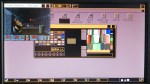
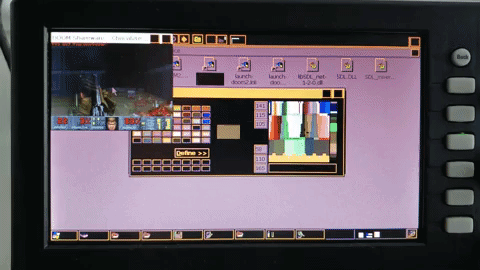
With the whole SPI Flash mapped out, I was able to, with much help from ChatGPT, make a couple custom tools: a Flash image splitter and repacker. I also used the Rinky-Dink UTFT library‘s conversion tools to enable replacement of the image data (i.e. custom theme support). Imagine that – custom theme/skin support on a vape, now a reality! With no help from the manufacturer!
-

- Flash dump splitter in action.
-

- Repacker tool in action.
Rationale
You might be asking: why anyone would do this? Honestly… I’m not sure; I just was fascinated by a colourful disposable vape and just had to thoroughly take it apart and learn everything I could about how it worked. Maybe this could give a reason for people to attempt to refill (and therefore reuse) their disposable vapes, and a reused vape is a vape that doesn’t end up in the landfill or roadside – and frankly, that’s good enough reason for me.
With the tooling set up, it was time for me to prove that these vapes can be rethemed, and I thought of a great retro aesthetic that is completely different from the original theme, yet easy for me to make with simple image editing tools: Windows 95.
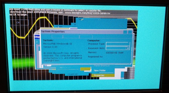
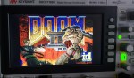
It runs Windows 95?!
Okay, not really… but I wanted a cohesive but entirely different theme to apply to the user interface, and I’m not nearly artistic enough to go about making a Doom theme (I tried, but couldn’t think of much that would work within the limitations of the original firmware). Using little more than a copy of Windows NT 4.0 (essentially the enterprise/professional version of Windows 95), some virtual machines, screenshot and recorder tools, and Microsoft Paint, I was able to create a UI that faithfully recreates the nostalgic Windows 95 user interface in a tiny 80×160 space.
Tip: if you need to frequently reprogram a device that uses an external (serial) memory chip, consider adding or making a socket for it. Additionally, vapes that use a 2-pin microphone element for inhalation sensing can be activated by shorting the pins to ground with a pushbutton, or even capacitively with your finger. If the vape requires a load to be present, a small halogen bulb will do the trick.
Main Screen
The main screen features the classic teal background, with two “windows” to represent the battery charge and vape juice levels. In keeping with Windows UI mechanics, the juice level is rendered as if it were an inactive window.
-

- 4x magnified simulation of the Windows 95 theme I created.
-

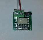
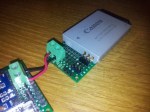
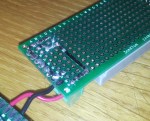
- A disassembled Kraze vape with socketed SPI Flash for easy testing.
-

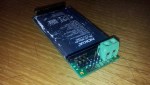
- Kraze HD7K turned into a development board with socketed Flash, test load and reset button.
Battery Level
The battery icon, while looking trivial to implement, required a lot of manual work to create the icons. From Windows 95 through XP, the default Windows UI’s battery icons were very limited in granularity: full, half, near empty, and empty. I had to employ “tweening” techniques by copying rows of pixels and aligning them to the desired levels, then manually painting in pixels where required. I also used a slightly more-detailed icon set from Windows XP which added a bit more of a highlight on the left side of the icon, rather than a flat blue colour. While it does somewhat detract from the “purity” of the icon set, the improved appearance was worth the tradeoff.
-

- 4x magnified simulation of the Windows 95 themed battery icon.
-

- Icon set pulled from Windows 95/NT 4.0’s systray.exe.
-

- Icon set pulled from Windows XP’s batmeter.dll.
Vape Juice Level
The juice level representation was a lot more challenging to conceive. I thought of using the Recycle Bin icon, but figured that making icons between empty and full wouldn’t produce a very unambiguous representation. I also thought about the magenta/blue pie chart used to represent disk usage, but that option was ruled out for similar ambiguity issues (I know that magenta is free space, and blue is used space, but this might not be intuitive enough without some sort of legend).
-

- 4x magnified simulation of the Windows 95 themed juice icon.
I finally figured that I had just enough room to make the world’s tiniest Explorer window, with just enough space for six 16×16 small icons. I picked a selection of icons that one would see in the C:\ root directory: folder, batch file, system file, application, .ini settings file, and unknown file (the one with a small Windows logo on it). As the vape juice is depleted, an icon is removed from the window. Once the juice is deemed by the microcontroller to be completely depleted, the blinking folder icon almost becomes homage to a similar phenomenon on Mac computers if it cannot find an operating system to boot.
Charging Animation
This one was another challenge, mainly due to the limited animation size of thirty 21×89 frames in an off-centre position atop a static background; not only that, the firmware dwells on the last animation for about a second, so any animation loop will need to stop cleanly at the last frame. The lack of animatable screen space meant that a file copy dialog was a non-starter, and the Windows 95 boot screen was also infeasible. I eventually settled on a small “Charging…” dialog box, with the animated hourglass cursor in the middle. One concession that I had to make was doubling each cursor animation frame, as well as losing one corner and edge of the hourglass during the initial animation sequence, as the hourglass is 22 pixels wide for the first few frames. Thankfully, this happens quickly enough that it isn’t particularly noticeable. I had pondered overlaying this dialog box atop the main UI’s “windows” but found the result to be too crowded in appearance, so a single dialog on the teal background was chosen instead.
-

- 4x magnified simulation of the charging animation. In reality this will not loop but instead goes to the main screen.
-

- The inverted colour area denotes what can be animated.
Vaping Animation
This one was arguably the most fun yet the most frustrating to actually implement. I knew I wanted to use a screensaver for the vaping animation, but which one? I needed a screensaver that was both iconic, but also looped cleanly. Flying Windows was a contender, but proved to scale down poorly and, due to its random nature, looped poorly as well. 3D Flower Box was skipped for the same reason (and wouldn’t have looked good looping once per second anyway). 3D Maze, 3D Text, and the simple graphic screensavers like Marquee, Mystify and Beziers were out too… so what’s left? Only one screensaver was left in the pipeline… a 3D pipeline – heh, get it? 😉 (sorry. I’ll see myself out for that joke.)
-

- A slightly slowed down simulation of the Windows 95 theme vaping animation I created.
-

- A screenshot of the 3D Pipes screensaver running in a VM, with a 1:2 aspect ratio.
3D Pipes is one of the most famous Windows 95-era screensavers, and despite its randomly-generated nature, had relatively clean transitions which make looping animations easier. It also scaled well both in terms of resolution and in time, but was an absolute pain to record. I eventually settled by running the Windows 95 version in a Windows XP virtual machine, with a custom screen size as close to a 1:2 aspect ratio as possible. After taking a screen recording, I had to then choose the sequence that looked the best, extract 16 frames from the video, scale those down to 80×160, and only then did I get my looped screensaver animation, but the result was well worth the effort. The particular run that I captured even had a flame-like shape to it!
Other Discoveries
With my main goal of extracting and replacing images on the vape accomplished, I decided to look further into its inner workings and learned a few things along the way.
A Secret Port
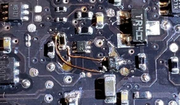
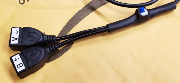
During my initial teardown, I noticed that the microcontroller’s SWD (Serial Wire Debug) programming lines were brought out to the USB-C port, but in an unusual way. The CC1/CC2 lines were not only used as regular 5.1k pulldowns to enable USB-C chargers to recognize the vape, but also as a programming connector. I had to build a custom cable to interface with it, but was able to use my Segger J-Link to communicate with the microcontroller in situ. As a bonus, the firmware is fully readable, without any encryption or readout prevention enabled!
-

- Custom-built debugging cable to debug vapes with SWD on the CC1/CC2 lines.
-

- Segger J-Link Commander is able to access the onboard microcontroller.
It’s Not About The Puffs
For a device marketed with a capacity of several thousands “puffs”, one would think that this would be tracked as a means to provide a vape juice gauge to the user. However, this turned out to not be the case, in more than one way.

The vape usage/time counter at exactly 10 seconds of usage. 0x3E8 = 1000, or 10.00 seconds.
Unlike many other disposable vape implementations, the juice meter’s data was stored in a non-volatile memory location, since neither a reset nor power cycle would reset the meter back to full. I was initially unsure where the microcontroller was holding this variable, and scanning the internal Flash memory and the extra few “option bytes” available above the usual firmware region showed no changes. It wasn’t until I decided to run a difference on the external SPI Flash between “puffs”, where I noticed bytes changing near location 0xF8000, in a sea of empty/0xFF bytes. Erasing the bytes from locations 0xF8000-0xF8004 resulted in the vape juice meter resetting back to full! Since vape inhalation sensors typically include a 10 second timeout, I decided to trigger a 10-second “puff” and noticed the memory location had updated to 0x3E8, which corresponds to 1000 in decimal. It was then easy to determine that the microcontroller was counting vape time with 0.01-second granularity.
A Beeline to the Buffer
Since I had access to the microcontroller’s memories in near-real time, I decided to experimentally determine where the data from the SPI Flash was getting copied into RAM. Since I already knew the microcontroller was using DMA to stream image data from the SPI Flash, I figured that I could fill its entire contents with human-readable text (in my case, I chose consecutive copies of the “Bee Movie” script) and observe the RAM’s contents changing in Segger J-Mem. This technique worked immediately, and it was obvious where the DMA buffer was held in RAM!
-

- Copies of the Bee Movie script in SPI flash showing up in a RAM buffer.
Blinking Power, Hidden Version (Screen)
Out of boredom and wanting to repeatedly test the charging animation during development, I was rapidly connecting and disconnecting power to the charging port. After several consecutive fast insertions and removals, I saw a black screen with red text pop up. It read “GV-K23 0904V1” and trying to capture it was difficult until I had the idea to use J-Link Commander to halt the CPU as soon as I triggered it. Given that the version screen had text, yet I saw no text strings in the firmware dump, I figured it had to be a bitmap image, and it was! It was stored near the very end of the firmware. While identifying where it was inside the dump was simple, trying to reconstruct it from the dump was not. The extra padding of 0x00 bytes (basically black when interpreted as RGB565) that didn’t align with 60 pixel/120-byte rows, it took a lot of experimentation with image sizes and offsets until I got a legible picture. Even now I’m still not entirely sure if I’ve captured the entire bitmap.
-

- Kraze vape showing its hidden version screen.
-

- 4x magnified visualization of the firmware flash dump, showing a scrambled version of the embedded version bitmap.
-

- 4x magnified reconstruction of the embedded version bitmap.
Further Efforts
In the time between me starting this reverse-engineering/modding project and my publication of this blog post, I released my documentation and rudimentary tools on my GitHub profile in the hopes of drumming up more support from the community. Within days, another GitHub user by the name of “xbenkozx” was able to apply and extend my research into the external Flash memory mapping and debugging facilities. He created his own Flash dumping and modding tools, and even built custom reflashing firmware that only needed access to a SWD debugging/programming dongle and a custom cable – no surface-mount soldering required (i.e. programming that is beyond my current skillset 🙂 ). He also made more detailed analyses of various board revisions, and some important incompatibilities that could have resulted in damage due to overheating of the vape’s heating coil. Check it out!
Hopefully this reverse-engineering and reuse campaign can branch even further. Perhaps development environments (maybe an Arduino board profile?) or alternative firmwares can be developed to allow these boards to be reused in other applications, given that these vapes already provide easy access to a bright LCD screen, a decently powerful Arm microcontroller, Li-ion battery charging, and a megabyte of SPI Flash storage plus some extra LED indicators. Some board versions even have Rx/Tx pads for a UART serial port, which could make communication between different devices a possibility.
In terms of just theme creation, I made an editable template on my GitHub repository, with example bar graphs and animation frames denoting positioning and frame count. Maybe someone out there with more graphics/artistic/programming talent than me could figure out a way to “run Doom” on these vapes! 😀
Conclusion
Disposable vapes are almost everywhere, and their wastefulness goes beyond just some rechargeable batteries and circuit boards – some have bright LCD screens… and yet somehow these are considered throwaway devices!
If you have some of these LCD-equipped disposable vapes like the Kraze HD7K or RAZ TN9000, perhaps try playing around with them a bit. I’ve spearheaded a community campaign on GitHub to reverse-engineer these vapes, which allows them to be reused or repurposed more easily. If you want to take the path of reuse, I and some others have made customization and reflashing tools available. There is also potential in reusing just the microcontroller board since the vape features a pretty powerful microcontroller and a lot of storage space for images.
-

- A Kraze HD7K disposable vape, modified with my custom Windows 95 theme. It is displaying a 3D Pipes screensaver animation.