As seen on Hackaday!
There’s always some electronics topic that I end up focusing all my efforts on (at least for a certain time), and that topic is now eMMC NAND Flash memory.
Overview
eMMC (sometimes shown as e.MMC or e-MMC) stands for Embedded MultiMediaCard; some manufacturers create their own name like SanDisk’s iNAND or Hynix’s e-NAND. It’s a very common form of Flash storage in smartphones and tablets, even lower-end laptops. The newer versions of the eMMC standard (4.5, 5.0 and 5.1) have placed greater emphasis on random small-block I/O (IOPS, or Input/Output operations per second; eMMC devices can now provide SSD-like performance (>10 MB/s 4KB read/write) without the higher cost and power consumption of a full SATA- or PCIe-based SSD.
MMC and eMMC storage is closely related to the SD card standard everyone knows today. In fact, SD hosts will often be able to use MMC devices without modification (electrically, they are the same, but software-wise SD has a slightly different feature set; for example SD cards have CPRM copy protection but lack the MMC’s TRIM and Secure Erase commands. The “e” in eMMC refers to the fact that the memory is a BGA chip directly soldered (embedded) to the motherboard (this also prevents it from being easily upgraded without the proper tools and know-how.
When browsing online for some eMMC chips to test out, I found a seller that had was selling 64 GB eMMC modules for $6 Canadian per pop; this comes out to a very nice 9.375 cents per gigabyte (that’s HDD-level pricing right there!). With that in mind, I decided to buy a couple modules and see what I could do with them. A few days later, they arrived in the mail (and the seller was nice enough to send three modules instead of just two; the third module’s solder balls were flattened for some reason).
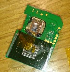
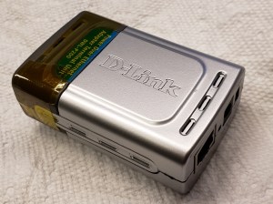
Toshiba eMMC Module

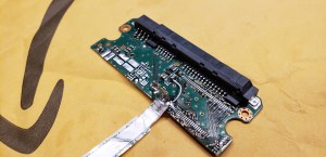
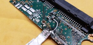
Toshiba THGBM4G9D8GBAII eMMC 4.41 modules
The Flash memory I used is a Toshiba THGBM4G9D8GBAII. According to a Toshiba NAND part number decoder:
- TH: Toshiba NAND
- G: Packaged as IC
- B: Vcc (Flash power supply) = 3.3 V, VccQ (controller/interface power supply) = 1.8 or 3.3 V
- M: eMMC device
- 4: Controller revision 4
- G9: 64 GB
- D: MLC NAND Flash
- 8: Eight stacked dice (eight 8 GB chips)
- G: 24nm A-type Flash (appears to indicate Toggle Mode interface NAND)
- BA: Lead-free and halogen-free
- I: Industrial temperature grade (-40 to 85 degrees Celsius)
- I: 14 x 18 x 1.2 mm BGA package with OSP (Organic Solderability Preservatives)
Given the low, low price of the eMMC chip, I had to make sure that I wasn’t given counterfeit Flash memory (often fake flash would have only 4 or 8 actual GB usable, with most of the address space looping over itself, causing data loss with extended usage). This involved find a way to temporarily connect the eMMC to my computer. I had a USB 2.0 SD/MMC reader on hand as well as a laptop with a native SD host interface, so now all I needed to do was break out the eMMC signals on the BGA package so that I can connect it to the reader.
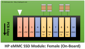
eMMC Pinout… or is it Ball-Out?
There are plenty of pinouts for eMMC on the Internet, but they all show the pinout for a top view. Since I’m not soldering the eMMC to a PCB, I need to get a bottom view. I took a pinout diagram from a SMART Modular Technologies eMMC datasheet, rotated it to a landscape view, flipped it vertically, then flipped each row’s text in order to make it readable again. I then copy-pasted this into PowerPoint and traced out the package and ball pinouts. This allowed me to colour-code the different signal and power lines I’ll need to implement, including the data, clock, command and power lines. Curiously enough, one of the ground pins (VssQ, or controller/MMC I/O ground) was not a ground pin like the standard required; because of this, I decided to leave that pin open-circuit. Additionally, there were several pins that were not open-circuit, but did not have a known purpose either (these are probably used as test pads for the internal NAND Flash interface – perhaps they could be reused as raw NAND with the right controller, but the exact purpose of these pads will need to be reverse engineered).

Toshiba THGBM4G9D8GBAII eMMC pinout (solder balls facing up)
eMMC Reader: Take 1 (Failed!)
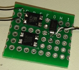
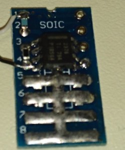
For the first reader, I cut open a microSD-to-SD adapter, exposing the eight pins inside. I soldered a cut-up UDMA IDE cable and glued them in place. Despite my careful work, I still melted a hole through the thin plastic shell of the adapter; thankfully this did not affect the adapter’s ability to be plugged in.
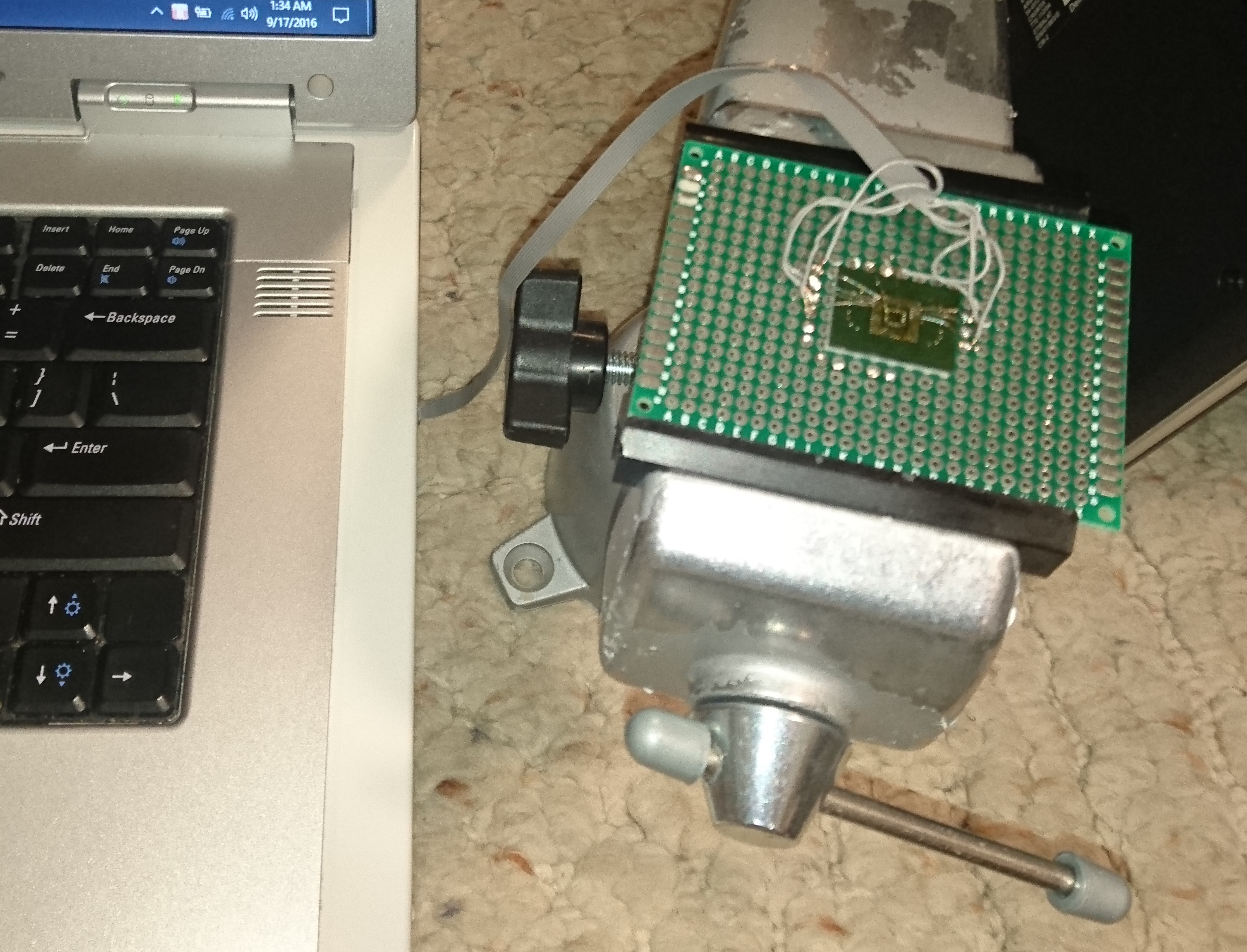
I used double-sided foam adhesive tape and a piece of perfboard to create a small “test bed” for the eMMC module. Using some flux, solder wick, and a larger soldering iron tip, I removed all the (lead-free) solder balls on the center of the IC and replaced them with leaded solder bumps to make soldering the tiny 40-gauge magnet wire easier.
After bringing out the minimum wires required (VCC/VCCQ, GND, CLK, CMD, and DAT0 for 1-bit operation), I soldered the wires of my quick SD adapter, and plugged it into the SD card slot of a (very old) Dell Inspiron 9300.
-
-
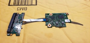
eMMC to SD adapter board, first attempt
-

-
First attempt of eMMC adapter plugged into laptop
Calling this board’s operation flaky doesn’t do it justice. It would fail to enumerate 9 out of 10 times, and if I even tried to do anything more than read the device capacity, the reader would hang or the eMMC would drop off the SD/MMC bus and show an empty drive in Windows. It was clear I had to do a full memory card “build” before I could verify the usability of the eMMC Flash memory.
eMMC in an SD Card’s Body: Take 1 (Success… half of the time)
I had a 16 MB (yes, megabyte) SD card lying around somewhere, but as usual, I couldn’t find it among all the clutter around my desk and workspace. Instead, I found an old, slow Kingston 2 GB SD card that I felt would be a worthy “sacrifice” since it was an older type that still had a thin PCB inside (most SD cards nowadays are monolithic, which means it’s one solid chunk with a few pads exposed). After opening up the case carefully with an Exacto knife, I wiggled out the old PCB. I desoldered the orignal 2 GB NAND Flash, and began work on breaking the SD card controller from the PCB as it was a chip-on-board design. It took a while, but I was able to ensure that none of the old SD card hardware would interfere with my rebuild.
-

-
SD card board with original Flash. Ironically we’re replacing Toshiba NAND with Toshiba eMMC.
-
-
eMMC attached and soldered to SD card PCB.
I removed the eMMC from the board I made previously, and tested the thickness of it to ensure that it would fit inside the SD card case. It did, although the 0402 surface-mount decoupling capacitors I intended to install would cause a few bumps to be visible through the thin plastic SD card casing.
With my eMMC and SD card pinouts on hand, I used a small bead of epoxy to affix the eMMC to the PCB, balls-side up. I used magnet wire to connect the data lines (4 wires for 4-bit operation which is the maximum that the SD standard supports), and used the unused pads on the eMMC as a kind of prototyping space where I could install ceramic capacitors as close to the module as possible. I used a 0.1 µF 0402 size ceramic capacitor across the VDDi (eMMC internal regulator) and a neighouring GND pad. The rest of the power pads were wired in parallel with a few extra 0.1 µF capacitors added. I made use of the existing three 1 µF capacitors on the PCB as both extra decoupling and connection points for VCC and VCCQ. To prevent shorting of the inner CMD and CLK pins, I only removed the enamel coating from the magnet wire at the very end so I could solder them but avoid the issue of shorting those pins against the other signal and power lines. I then soldered these wires to the terminals on the other side of the PCB.
After spending about ten minutes wriggling the PCB into the SD card casing without damaging the wires, I used a multimeter to ensure all the pins were connected (use a multimeter in diode mode, with the positive lead connected to ground – any valid pins should read ~0.5 volts), and also ensured that there were no polarity reversals or shorts on the power pins.
Now… the moment of truth. At this point my USB 2.0 card reader still wasn’t cooperating with me, so I tried the only other ‘fast’ reader I had at the time – an SD to CompactFlash adapter.
-
-
eMMC in SD-to-CF adapter visible
-
-
eMMC MBR
To my relief, I finally got a (mostly) usable card. It appears this particular model has been pre-formatted with FAT32. Viewing the MBR in Hard Disk Sentinel shows nothing notable, apart from the fact that it’s pretty blank and is indicative that it wasn’t formatted for use as a PC boot medium.
Things began to fall apart after I tried running speed tests, as the card would hang if it experienced a lot of write activity at once. I suspected this was a power supply-related issue, so I modified my layout to add more capacitance. For good measure, I added 56 ohm termination resistance for the DAT0-4 data lines, using a small resistor network harvested from an old dead MacBook motherboard.
After these modifications, performance was much, much better. Now that the card was usable, I could finally run some speed tests.
eMMC in an SD Card’s Body – This time, with more feeling decoupling!
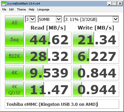
After adding several 100 nF and 1uF 0402-size ceramic capacitors on the eMMC package, I was able to get a stable card that could be read by (most) SD card readers. As I was rather anxious to get a decent benchmark from the eMMC, I decided to forego the cheaper Amazon Prime route, and go to my local PC parts store to buy a USB 3.0 card reader – the Kingston FCR-HS4.
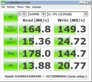
After placing the eMMC and SD card PCB back into its plastic casing, I was relieved to see that Windows immediately recognized its presence. All I had to do then was open CrystalDiskMark and run the benchmark. Drum roll please…

Toshiba THGBM4G9D8GBAII/064G4A benchmark in CrystalDiskMark
Although I was happy to get a usable benchmark score, my belief that all eMMC devices inherently had better 4K random I/O speeds than their SD counterparts was immediately busted. My guess is that random I/O wasn’t considered to be a priority until eMMC 4.5 or 5.0, and my eMMC modules are only version 4.41.

eMMC module listed as version 4.41
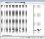
After the speed test, I ran the card through the popular Flash memory testing tool h2testw to make sure that I was not given a counterfeit device.

H2testw showing flash memory is good
Excellent – it’s a genuine device. Despite the slower performance than expected, I’m happy that the memory capacity is as it should be.
“eMMC identification and CSD data, please”
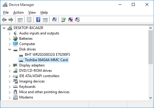
As is the case with any USB memory card reader, I cannot access any of the eMMC device information (that is, the CID/Card Information Data and CSD/Card Specific Data registers). I took a spare SSD from my collection and got a quick Windows 10 installation running on one of my laptops that had a native SD host interface.
eMMC identified as Toshiba 064G4A MMC
Interesting. The eMMC identifies itself as a Toshiba 064G4A MMC card. Googling that information brought up literally zero information, so it appears I’m the only one to have found (or published) any information about it. Although eMMCs support some degree of S.M.A.R.T. health reporting like mainstream SSDs and HDDs, no (easily-available) software (for Windows at least) is available to read it.
Linux has the ability to report the CID and CSD data as long as the native SD host interface is used, as opposed to a USB card reader.
CID: 11010030363447344100151344014e00
CSD: d00e00320f5903ffffffffef96400000
date: 04/2011
enhanced_area_offset: 18446744073709551594
erase_size: 8388608
fwrev: 0x0
hwrev: 0x0
manfid: 0x000011
oemid: 0x0100
preferred_erase_size: 8388608
prv: 0x0
raw_rpmb_size_mult: 0x2
rel_sectors: 0x10
serial: 0x15134401
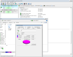
With the help of Gough Lui’s CID and CSD decoders, I was able to gain some more information about the eMMC device, but not too much as the information I was originally interested in was already collected by this point.
-

-
eMMC CID decoded with Gough Lui’s online tool
Out of the Reader and Back Into the (CF) Adapter
Now that I know what the eMMC is capable of, I decided to try putting it back into my SD-to-CF adapter and doing another benchmark.
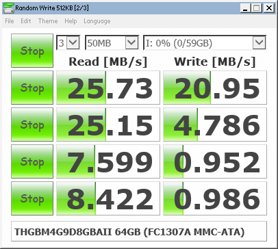
eMMC in FC-1307A SD-to-CF adapter. Note the limited performance of this chipset.
This test highlights one of the biggest limitations of the FC1306T/FC1307A chipset that so many adapters use: their performance is limited to a maximum of 25 MB/s per channel. Good thing I purchased that USB 3.0 reader…
Conclusion
This was quite the learning experience. I not only learned that eMMC flash memory does not necessarily have the near-SSD performance that the latest devices offer, but I learned how to “exploit” the unused pads of a BGA device as a sort of “prototype area” for soldering small components onto.
Did I save any money by rolling my own Flash storage device? Absolutely not – given how much time I spent on this, if I paid myself minimum wage ($12 per hour where I live), I could have bought at least three higher-performance 64GB SDXC cards with none of the frustration of trying to adapt an embedded memory device as a removable memory card. But where’s the fun in that? 🙂


")
")